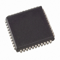
AT89C51RD2-SLSUM Atmel, AT89C51RD2-SLSUM Datasheet - Page 71

AT89C51RD2-SLSUM
Manufacturer Part Number
AT89C51RD2-SLSUM
Description
IC 8051 MCU FLASH 64K 44PLCC
Manufacturer
Atmel
Series
89Cr
Datasheet
1.ATWEBDVK-02RC.pdf
(137 pages)
Specifications of AT89C51RD2-SLSUM
Core Processor
8051
Core Size
8-Bit
Speed
60MHz
Connectivity
SPI, UART/USART
Peripherals
POR, PWM, WDT
Number Of I /o
34
Program Memory Size
64KB (64K x 8)
Program Memory Type
FLASH
Ram Size
2K x 8
Voltage - Supply (vcc/vdd)
2.7 V ~ 5.5 V
Oscillator Type
External
Operating Temperature
-40°C ~ 85°C
Package / Case
44-PLCC
Processor Series
AT89x
Core
8051
Data Bus Width
8 bit
Data Ram Size
2 KB
Interface Type
UART, SPI
Maximum Clock Frequency
60 MHz
Number Of Programmable I/os
32
Number Of Timers
3
Operating Supply Voltage
2.7 V to 5.5 V
Maximum Operating Temperature
+ 85 C
Mounting Style
SMD/SMT
3rd Party Development Tools
PK51, CA51, A51, ULINK2
Minimum Operating Temperature
- 40 C
Package
44PLCC
Device Core
80C51
Family Name
89C
Maximum Speed
40 MHz
For Use With
AT89OCD-01 - USB EMULATOR FOR AT8XC51 MCUAT89STK-11 - KIT STARTER FOR AT89C51RX2
Lead Free Status / RoHS Status
Lead free / RoHS Compliant
Eeprom Size
-
Data Converters
-
Lead Free Status / Rohs Status
Details
Available stocks
Company
Part Number
Manufacturer
Quantity
Price
Company:
Part Number:
AT89C51RD2-SLSUM
Manufacturer:
ATMEL
Quantity:
185 248
Company:
Part Number:
AT89C51RD2-SLSUM
Manufacturer:
CMD
Quantity:
1 993
Part Number:
AT89C51RD2-SLSUM
Manufacturer:
MICROCHIP/微芯
Quantity:
20 000
16.3.5.3
4235K–8051–05/08
Serial Peripheral DATa Register (SPDAT)
Reset Value = 00X0 XXXXb
Not Bit addressable
The Serial Peripheral Data Register
ter. A write to SPDAT places data directly into the shift register. No transmit buffer is available in
this model.
A Read of the SPDAT returns the value located in the receive buffer and not the content of the
shift register.
Table 16-5.
SPDAT - Serial Peripheral Data Register (0C5H)
Reset Value = Indeterminate
R7:R0: Receive data bits
SPCON, SPSTA and SPDAT registers may be read and written at any time while there is no on-
going exchange. However, special care should be taken when writing to them while a transmis-
sion is on-going:
Bit Number
• Do not change SPR2, SPR1 and SPR0
• Do not change CPHA and CPOL
• Do not change MSTR
• Clearing SPEN would immediately disable the peripheral
• Writing to the SPDAT will cause an overflow.
R7
5
4
3
2
1
0
7
Mnemonic
SSERR
SPDAT Register
MODF
Bit
R6
-
-
-
-
6
Description
Synchronous Serial Slave Error Flag
Set by hardware when SS is de-asserted before the end of a received data.
Cleared by disabling the SPI (clearing SPEN bit in SPCON).
Mode Fault
Cleared by hardware to indicate that the SS pin is at appropriate logic level, or has been
approved by a clearing sequence.
Set by hardware to indicate that the SS pin is at inappropriate logic level.
Reserved
The value read from this bit is indeterminate. Do not set this bit
Reserved
The value read from this bit is indeterminate. Do not set this bit.
Reserved
The value read from this bit is indeterminate. Do not set this bit.
Reserved
The value read from this bit is indeterminate. Do not set this bit.
R5
5
(Table
R4
4
16-5) is a read/write buffer for the receive data regis-
R3
3
AT89C51RD2/ED2
R2
2
R1
1
R0
0
71


