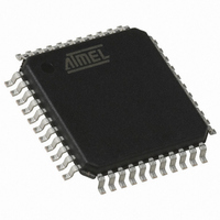
AT89C51CC03CA-RLTUM Atmel, AT89C51CC03CA-RLTUM Datasheet - Page 129

AT89C51CC03CA-RLTUM
Manufacturer Part Number
AT89C51CC03CA-RLTUM
Description
IC 8051 MCU 64K FLASH 44-VQFP
Manufacturer
Atmel
Series
AT89C CANr
Datasheet
1.AT89C51CC03C-S3RIM.pdf
(198 pages)
Specifications of AT89C51CC03CA-RLTUM
Core Processor
8051
Core Size
8-Bit
Speed
40MHz
Connectivity
CAN, UART/USART
Peripherals
POR, PWM, WDT
Number Of I /o
36
Program Memory Size
64KB (64K x 8)
Program Memory Type
FLASH
Eeprom Size
2K x 8
Ram Size
2.25K x 8
Voltage - Supply (vcc/vdd)
3 V ~ 5.5 V
Data Converters
A/D 8x10b
Oscillator Type
External
Operating Temperature
-40°C ~ 85°C
Package / Case
44-TQFP, 44-VQFP
Processor Series
AT89x
Core
8051
Data Bus Width
8 bit
Data Ram Size
2304 B
Interface Type
UART, SPI
Maximum Clock Frequency
60 MHz
Number Of Programmable I/os
36
Number Of Timers
2
Operating Supply Voltage
3 V to 5.5 V
Maximum Operating Temperature
+ 85 C
Mounting Style
SMD/SMT
3rd Party Development Tools
PK51, CA51, A51, ULINK2
Minimum Operating Temperature
- 40 C
On-chip Adc
10 bit, 8 Channel
Package
44VQFP
Device Core
8051
Family Name
AT89
Maximum Speed
60 MHz
For Use With
AT89OCD-01 - USB EMULATOR FOR AT8XC51 MCU
Lead Free Status / RoHS Status
Lead free / RoHS Compliant
Available stocks
Company
Part Number
Manufacturer
Quantity
Price
Company:
Part Number:
AT89C51CC03CA-RLTUM
Manufacturer:
ADI
Quantity:
141
Serial Port Interface
(SPI)
Features
Signal Description
Master Output Slave Input
(MOSI)
Master Input Slave Output
(MISO)
SPI Serial Clock (SCK)
Slave Select (SS)
4182O–CAN–09/08
The Serial Peripheral Interface Module (SPI) allows full-duplex, synchronous, serial
communication between the MCU and peripheral devices, including other MCUs.
Features of the SPI Module include the following:
•
•
•
•
•
Figure 57 shows a typical SPI bus configuration using one Master controller and many
Slave peripherals. The bus is made of three wires connecting all the devices.
Figure 57. SPI Master/Slaves Interconnection
The Master device selects the individual Slave devices by using four pins of a parallel
port to control the four SS pins of the Slave devices.
This 1-bit signal is directly connected between the Master Device and a Slave Device.
The MOSI line is used to transfer data in series from the Master to the Slave. Therefore,
it is an output signal from the Master, and an input signal to a Slave. A Byte (8-bit word)
is transmitted most significant bit (MSB) first, least significant bit (LSB) last.
This 1-bit signal is directly connected between the Slave Device and a Master Device.
The MISO line is used to transfer data in series from the Slave to the Master. Therefore,
it is an output signal from the Slave, and an input signal to the Master. A Byte (8-bit
word) is transmitted most significant bit (MSB) first, least significant bit (LSB) last.
This signal is used to synchronize the data transmission both in and out of the devices
through their MOSI and MISO lines. It is driven by the Master for eight clock cycles
which allows to exchange one Byte on the serial lines.
Each Slave peripheral is selected by one Slave Select pin (SS). This signal must stay
low for any message for a Slave. It is obvious that only one Master (SS high level) can
drive the network. The Master may select each Slave device by software through port
pins (Figure 58). To prevent bus conflicts on the MISO line, only one slave should be
selected at a time by the Master for a transmission.
Full-duplex, three-wire synchronous transfers
Master or Slave operation
Six programmable Master clock rates in master mode
Serial clock with programmable polarity and phase
Master Mode fault error flag with MCU interrupt capability
Master
Slave 4
MISO
MOSI
SCK
SS
0
1
2
3
VDD
Slave 3
AT89C51CC03
Slave 1
Slave 2
129


