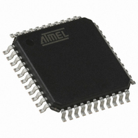
AT89C51CC03CA-RLTUM Atmel, AT89C51CC03CA-RLTUM Datasheet - Page 17

AT89C51CC03CA-RLTUM
Manufacturer Part Number
AT89C51CC03CA-RLTUM
Description
IC 8051 MCU 64K FLASH 44-VQFP
Manufacturer
Atmel
Series
AT89C CANr
Datasheet
1.AT89C51CC03C-S3RIM.pdf
(198 pages)
Specifications of AT89C51CC03CA-RLTUM
Core Processor
8051
Core Size
8-Bit
Speed
40MHz
Connectivity
CAN, UART/USART
Peripherals
POR, PWM, WDT
Number Of I /o
36
Program Memory Size
64KB (64K x 8)
Program Memory Type
FLASH
Eeprom Size
2K x 8
Ram Size
2.25K x 8
Voltage - Supply (vcc/vdd)
3 V ~ 5.5 V
Data Converters
A/D 8x10b
Oscillator Type
External
Operating Temperature
-40°C ~ 85°C
Package / Case
44-TQFP, 44-VQFP
Processor Series
AT89x
Core
8051
Data Bus Width
8 bit
Data Ram Size
2304 B
Interface Type
UART, SPI
Maximum Clock Frequency
60 MHz
Number Of Programmable I/os
36
Number Of Timers
2
Operating Supply Voltage
3 V to 5.5 V
Maximum Operating Temperature
+ 85 C
Mounting Style
SMD/SMT
3rd Party Development Tools
PK51, CA51, A51, ULINK2
Minimum Operating Temperature
- 40 C
On-chip Adc
10 bit, 8 Channel
Package
44VQFP
Device Core
8051
Family Name
AT89
Maximum Speed
60 MHz
For Use With
AT89OCD-01 - USB EMULATOR FOR AT8XC51 MCU
Lead Free Status / RoHS Status
Lead free / RoHS Compliant
Available stocks
Company
Part Number
Manufacturer
Quantity
Price
Company:
Part Number:
AT89C51CC03CA-RLTUM
Manufacturer:
ADI
Quantity:
141
Clock
Description
4182O–CAN–09/08
The AT89C51CC03 core needs only 6 clock periods per machine cycle. This feature,
called”X2”, provides the following advantages:
•
•
•
•
In order to keep the original C51 compatibility, a divider-by-2 is inserted between the
XTAL1 signal and the main clock input of the core (phase generator). This divider may
be disabled by the software.
An extra feature is available to start after Reset in the X2 mode. This feature can be
enabled by a bit X2B in the Hardware Security Byte. This bit is described in the section
"In-System Programming".
The X2 bit in the CKCON register (see Table 2) allows switching from 12 clock cycles
per instruction to 6 clock cycles and vice versa. At reset, the standard speed is activated
(STD mode).
Setting this bit activates the X2 feature (X2 mode) for the CPU Clock only (see Figure
5.).
The Timers 0, 1 and 2, Uart, PCA, WatchDog or CAN switch in X2 mode only if the cor-
responding bit is cleared in the CKCON register.
The clock for the whole circuit and peripheral is first divided by two before being used by
the CPU core and peripherals. This allows any cyclic ratio to be accepted on the XTAL1
input. In X2 mode, as this divider is bypassed, the signals on XTAL1 must have a cyclic
ratio between 40 to 60%. Figure 5. shows the clock generation block diagram. The X2
bit is validated on the XTAL1÷2 rising edge to avoid glitches when switching from the X2
to the STD mode. Figure 6 shows the mode switching waveforms.
Divides frequency crystals by 2 (cheaper crystals) while keeping the same CPU
power.
Saves power consumption while keeping the same CPU power (oscillator power
saving).
Saves power consumption by dividing dynamic operating frequency by 2 in
operating and idle modes.
Increases CPU power by 2 while keeping the same crystal frequency.
AT89C51CC03
17


