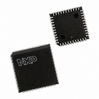
P89LV51RD2FA,512 NXP Semiconductors, P89LV51RD2FA,512 Datasheet - Page 21

P89LV51RD2FA,512
Manufacturer Part Number
P89LV51RD2FA,512
Description
IC 80C51 MCU 1024 RAM 44PLCC
Manufacturer
NXP Semiconductors
Series
89LVr
Datasheet
1.P89LV51RD2BBC557.pdf
(76 pages)
Specifications of P89LV51RD2FA,512
Core Processor
8051
Core Size
8-Bit
Speed
33MHz
Connectivity
SPI, UART/USART
Peripherals
Brown-out Detect/Reset, POR, PWM, WDT
Number Of I /o
32
Program Memory Size
64KB (64K x 8)
Program Memory Type
FLASH
Ram Size
1K x 8
Voltage - Supply (vcc/vdd)
2.7 V ~ 3.6 V
Oscillator Type
Internal
Operating Temperature
-40°C ~ 85°C
Package / Case
44-PLCC
Processor Series
P89LV5x
Core
80C51
Data Bus Width
8 bit
Data Ram Size
1 KB
Interface Type
SPI, UART
Maximum Clock Frequency
33 MHz
Number Of Programmable I/os
32
Number Of Timers
3
Operating Supply Voltage
2.4 V to 3.6 V
Maximum Operating Temperature
+ 85 C
Mounting Style
SMD/SMT
3rd Party Development Tools
PK51, CA51, A51, ULINK2
Minimum Operating Temperature
- 40 C
Package
44PLCC
Device Core
80C51
Family Name
89LV
Maximum Speed
40 MHz
For Use With
622-1017 - BOARD 44-ZIF PLCC SOCKET622-1008 - BOARD FOR LPC9103 10-HVSON
Lead Free Status / RoHS Status
Lead free / RoHS Compliant
Eeprom Size
-
Data Converters
-
Lead Free Status / Rohs Status
Details
Other names
935274176512
P89LV51RD2FA
P89LV51RD2FA
P89LV51RD2FA
P89LV51RD2FA
Available stocks
Company
Part Number
Manufacturer
Quantity
Price
Company:
Part Number:
P89LV51RD2FA,512
Manufacturer:
NXP Semiconductors
Quantity:
10 000
Part Number:
P89LV51RD2FA,512
Manufacturer:
NXP/恩智浦
Quantity:
20 000
NXP Semiconductors
P89LV51RB2_RC2_RD2_5
Product data sheet
6.3.3 ISP
6.3.4 Using ISP
A chip-erase operation can be performed using a commercially available parallel
programer. This operation will erase the contents of this boot block and it will be
necessary for the user to reprogram this boot block (block 1) with the NXP-provided
ISP/IAP code in order to use the ISP or IAP capabilities of this device. Go to
http://www.nxp.com/support
ISP is performed without removing the microcontroller from the system. The ISP facility
consists of a series of internal hardware resources coupled with internal firmware to
facilitate remote programming of the P89LV51RB2/RC2/RD2 through the serial port. This
firmware is provided by NXP and embedded within each P89LV51RB2/RC2/RD2 device.
The NXP ISP facility has made in-circuit programming in an embedded application
possible with a minimum of additional expense in components and circuit board area. The
ISP function uses five pins (V
needs to be available to interface your application to an external circuit in order to use this
feature.
The ISP feature allows for a wide range of baud rates to be used in your application,
independent of the oscillator frequency. It is also adaptable to a wide range of oscillator
frequencies. This is accomplished by measuring the bit-time of a single bit in a received
character. This information is then used to program the baud rate in terms of timer counts
based on the oscillator frequency. The ISP feature requires that an initial character (an
uppercase U) be sent to the P89LV51RB2/RC2/RD2 to establish the baud rate. The ISP
firmware provides auto-echo of received characters. Once baud rate initialization has
been performed, the ISP firmware will only accept Intel Hex-type records. Intel Hex
records consist of ASCII characters used to represent hexadecimal values and are
summarized below:
In the Intel Hex record, the ‘NN’ represents the number of data bytes in the record. The
P89LV51RB2/RC2/RD2 will accept up to 32 data bytes. The ‘AAAA’ string represents the
address of the first byte in the record. If there are zero bytes in the record, this field is often
set to 0000. The ‘RR’ string indicates the record type. A record type of ‘00’ is a data
record. A record type of ‘01’ indicates the end-of-file mark. In this application, additional
record types will be added to indicate either commands or data for the ISP facility.
The maximum number of data bytes in a record is limited to 32 (decimal). ISP commands
are summarized in
information in the record is stored internally and a checksum calculation is performed. The
operation indicated by the record type is not performed until the entire record has been
received. Should an error occur in the checksum, the P89LV51RB2/RC2/RD2 will send an
‘X’ out the serial port indicating a checksum error. If the checksum calculation is found to
match the checksum in the record, then the command will be executed. In most cases,
successful reception of the record will be indicated by transmitting a ‘.’ character out the
serial port.
:NNAAAARRDD..DDCC<crlf>
Table
Rev. 05 — 15 December 2009
12. As a record is received by the P89LV51RB2/RC2/RD2, the
for questions or to obtain the hex file for this device.
DD
, V
SS
, TXD, RXD, and RST). Only a small connector
P89LV51RB2/RC2/RD2
8-bit microcontrollers with 80C51 core
© NXP B.V. 2009. All rights reserved.
21 of 76


