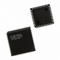
P89LV51RD2FA,512 NXP Semiconductors, P89LV51RD2FA,512 Datasheet - Page 29

P89LV51RD2FA,512
Manufacturer Part Number
P89LV51RD2FA,512
Description
IC 80C51 MCU 1024 RAM 44PLCC
Manufacturer
NXP Semiconductors
Series
89LVr
Datasheet
1.P89LV51RD2BBC557.pdf
(76 pages)
Specifications of P89LV51RD2FA,512
Core Processor
8051
Core Size
8-Bit
Speed
33MHz
Connectivity
SPI, UART/USART
Peripherals
Brown-out Detect/Reset, POR, PWM, WDT
Number Of I /o
32
Program Memory Size
64KB (64K x 8)
Program Memory Type
FLASH
Ram Size
1K x 8
Voltage - Supply (vcc/vdd)
2.7 V ~ 3.6 V
Oscillator Type
Internal
Operating Temperature
-40°C ~ 85°C
Package / Case
44-PLCC
Processor Series
P89LV5x
Core
80C51
Data Bus Width
8 bit
Data Ram Size
1 KB
Interface Type
SPI, UART
Maximum Clock Frequency
33 MHz
Number Of Programmable I/os
32
Number Of Timers
3
Operating Supply Voltage
2.4 V to 3.6 V
Maximum Operating Temperature
+ 85 C
Mounting Style
SMD/SMT
3rd Party Development Tools
PK51, CA51, A51, ULINK2
Minimum Operating Temperature
- 40 C
Package
44PLCC
Device Core
80C51
Family Name
89LV
Maximum Speed
40 MHz
For Use With
622-1017 - BOARD 44-ZIF PLCC SOCKET622-1008 - BOARD FOR LPC9103 10-HVSON
Lead Free Status / RoHS Status
Lead free / RoHS Compliant
Eeprom Size
-
Data Converters
-
Lead Free Status / Rohs Status
Details
Other names
935274176512
P89LV51RD2FA
P89LV51RD2FA
P89LV51RD2FA
P89LV51RD2FA
Available stocks
Company
Part Number
Manufacturer
Quantity
Price
Company:
Part Number:
P89LV51RD2FA,512
Manufacturer:
NXP Semiconductors
Quantity:
10 000
Part Number:
P89LV51RD2FA,512
Manufacturer:
NXP/恩智浦
Quantity:
20 000
NXP Semiconductors
P89LV51RB2_RC2_RD2_5
Product data sheet
6.4.1 Mode 0
6.4.2 Mode 1
Table 18.
Putting either Timer into mode 0 makes it look like an 8048 Timer, which is an 8-bit
counter with a fixed divide-by-32 prescaler.
In this mode, the Timer register is configured as a 13-bit register. As the count rolls over
from all 1s to all 0s, it sets the Timer interrupt flag TFn. The count input is enabled to the
Timer when TRn = 1 and either GATE = 0 or INTn = 1. Setting GATE = 1 allows the Timer
to be controlled by external input INTn, to facilitate pulse width measurements. TRn is a
control bit in the Special Function Register TCON
register.
The 13-bit register consists of all 8 bits of THn and the lower 5 bits of TLn. The upper
3 bits of TLn are indeterminate and should be ignored. Setting the run flag (TRn) does not
clear the registers.
Mode 0 operation is the same for Timer 0 and Timer 1 (see
different GATE bits, one for Timer 1 (TMOD.7) and one for Timer 0 (TMOD.3).
Mode 1 is the same as mode 0, except that all 16 bits of the timer register (THn and TLn)
are used. See
Bit
2
1
0
Fig 7. Timer/counter 0 or 1 in mode 0 (13-bit counter)
INTn pin
TnGate
Tn pin
osc/6
TRn
TCON - Timer/counter control register (address 88H) bit descriptions
Symbol
IT1
IE0
IT0
Figure
Rev. 05 — 15 December 2009
8.
Description
Interrupt 1 Type control bit. Set/cleared by software to specify falling
edge/low level that triggers external interrupt 1.
Interrupt 0 Edge flag. Set by hardware when external interrupt 0
edge/low level is detected. Cleared by hardware when the interrupt is
processed, or by software.
Interrupt 0 Type control bit. Set/cleared by software to specify falling
edge/low level that triggers external interrupt 0.
C/T = 0
C/T = 1
P89LV51RB2/RC2/RD2
control
Figure 7
8-bit microcontrollers with 80C51 core
(Figure
(5-bits)
TLn
shows mode 0 operation.
6). The GATE bit is in the TMOD
(8-bits)
THn
Figure
overflow
7). There are two
© NXP B.V. 2009. All rights reserved.
TFn
002aaa519
…continued
interrupt
29 of 76


