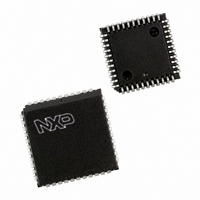
P89LV51RD2FA,512 NXP Semiconductors, P89LV51RD2FA,512 Datasheet - Page 40

P89LV51RD2FA,512
Manufacturer Part Number
P89LV51RD2FA,512
Description
IC 80C51 MCU 1024 RAM 44PLCC
Manufacturer
NXP Semiconductors
Series
89LVr
Datasheet
1.P89LV51RD2BBC557.pdf
(76 pages)
Specifications of P89LV51RD2FA,512
Core Processor
8051
Core Size
8-Bit
Speed
33MHz
Connectivity
SPI, UART/USART
Peripherals
Brown-out Detect/Reset, POR, PWM, WDT
Number Of I /o
32
Program Memory Size
64KB (64K x 8)
Program Memory Type
FLASH
Ram Size
1K x 8
Voltage - Supply (vcc/vdd)
2.7 V ~ 3.6 V
Oscillator Type
Internal
Operating Temperature
-40°C ~ 85°C
Package / Case
44-PLCC
Processor Series
P89LV5x
Core
80C51
Data Bus Width
8 bit
Data Ram Size
1 KB
Interface Type
SPI, UART
Maximum Clock Frequency
33 MHz
Number Of Programmable I/os
32
Number Of Timers
3
Operating Supply Voltage
2.4 V to 3.6 V
Maximum Operating Temperature
+ 85 C
Mounting Style
SMD/SMT
3rd Party Development Tools
PK51, CA51, A51, ULINK2
Minimum Operating Temperature
- 40 C
Package
44PLCC
Device Core
80C51
Family Name
89LV
Maximum Speed
40 MHz
For Use With
622-1017 - BOARD 44-ZIF PLCC SOCKET622-1008 - BOARD FOR LPC9103 10-HVSON
Lead Free Status / RoHS Status
Lead free / RoHS Compliant
Eeprom Size
-
Data Converters
-
Lead Free Status / Rohs Status
Details
Other names
935274176512
P89LV51RD2FA
P89LV51RD2FA
P89LV51RD2FA
P89LV51RD2FA
Available stocks
Company
Part Number
Manufacturer
Quantity
Price
Company:
Part Number:
P89LV51RD2FA,512
Manufacturer:
NXP Semiconductors
Quantity:
10 000
Part Number:
P89LV51RD2FA,512
Manufacturer:
NXP/恩智浦
Quantity:
20 000
NXP Semiconductors
P89LV51RB2_RC2_RD2_5
Product data sheet
6.6.8 Multiprocessor communications
6.6.9 Automatic address recognition
The signal to load SBUF and RB8, and to set RI, will be generated if, and only if, the
following conditions are met at the time the final shift pulse is generated: (a) RI = 0, and
(b) either SM2 = 0, or the received 9th data bit = 1.
If either of these conditions is not met, the received frame is irretrievably lost, and RI is not
set. If both conditions are met, the received 9th data bit goes into RB8, and the first 8 data
bits go into SBUF.
UART modes 2 and 3 have a special provision for multiprocessor communications. In
these modes, 9 data bits are received or transmitted. When data is received, the 9th bit is
stored in RB8. The UART can be programmed so that when the stop bit is received, the
serial port interrupt will be activated only if RB8 = 1. This feature is enabled by setting bit
SM2 in SCON. One way to use this feature in multiprocessor systems is as follows:
When the master processor wants to transmit a block of data to one of several slaves, it
first sends out an address byte which identifies the target slave. An address byte differs
from a data byte in a way that the 9th bit is ‘1’ in an address byte and ‘0’ in the data byte.
With SM2 = 1, no slave will be interrupted by a data byte, i.e. the received 9th bit is ‘0’.
However, an address byte having the 9th bit set to ‘1’ will interrupt all slaves, so that each
slave can examine the received byte and see if it is being addressed or not. The
addressed slave will clear its SM2 bit and prepare to receive the data (still 9 bits long) that
follow. The slaves that weren’t being addressed leave their SM2 bits set and ignore the
subsequent data bytes.
SM2 has no effect in mode 0, and in mode 1 can be used to check the validity of the stop
bit, although this is better done with the Framing Error flag. When the UART receives data
in mode 1 and SM2 = 1, the receive interrupt will not be activated unless a valid stop bit is
received.
Automatic Address Recognition is a feature which allows the UART to recognize certain
addresses in the serial bit stream by using hardware to make the comparisons. This
feature saves a great deal of software overhead by eliminating the need for the software to
examine every serial address which passes by the serial port. This feature is enabled for
the UART by setting the SM2 bit in SCON. In the 9 bit UART modes, mode 2 and mode 3,
the Receive Interrupt flag (RI) will be automatically set when the received byte contains
either the ‘Given’ address or the ‘Broadcast' address. The 9 bit mode requires that the 9th
information bit is a ‘1’ to indicate that the received information is an address and not data.
Using the Automatic Address Recognition feature allows a master to selectively
communicate with one or more slaves by invoking the Given slave address or addresses.
All of the slaves may be contacted by using the Broadcast address. Two Special Function
Registers are used to define the slave’s address, SADDR, and the address mask,
SADEN. SADEN is used to define which bits in the SADDR are to be used and which bits
are ‘don’t care’. The SADEN mask can be logically ANDed with the SADDR to create the
‘Given’ address which the master will use for addressing each of the slaves. Use of the
Given address allows multiple slaves to be recognized while excluding others.
This device uses the methods presented in
‘Broadcast’ address has been received or not.
Rev. 05 — 15 December 2009
P89LV51RB2/RC2/RD2
Figure 15
8-bit microcontrollers with 80C51 core
to determine if a ‘Given’ or
© NXP B.V. 2009. All rights reserved.
40 of 76


