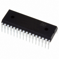
ST72F264G2B6 STMicroelectronics, ST72F264G2B6 Datasheet - Page 129

ST72F264G2B6
Manufacturer Part Number
ST72F264G2B6
Description
MCU 8-BIT 8K FLASH 32-SDIP
Manufacturer
STMicroelectronics
Series
ST7r
Specifications of ST72F264G2B6
Mfg Application Notes
ST7 Checksum Capability, AN1070 App Note
Core Processor
ST7
Core Size
8-Bit
Speed
16MHz
Connectivity
I²C, SCI, SPI
Peripherals
LVD, POR, PWM, WDT
Number Of I /o
22
Program Memory Size
8KB (8K x 8)
Program Memory Type
FLASH
Ram Size
256 x 8
Voltage - Supply (vcc/vdd)
2.7 V ~ 5.5 V
Data Converters
A/D 6x10b
Oscillator Type
Internal
Operating Temperature
-40°C ~ 85°C
Package / Case
32-SDIP (0.400", 10.16mm)
Processor Series
ST72F2x
Core
ST7
Data Bus Width
8 bit
Data Ram Size
256 B
Interface Type
I2C, SCI, SPI
Maximum Clock Frequency
8 MHz
Number Of Programmable I/os
22
Number Of Timers
3
Maximum Operating Temperature
+ 85 C
Mounting Style
Through Hole
Development Tools By Supplier
ST7F264-IND/USB, ST72F34X-SK/RAIS, ST7MDT10-DVP3, ST7MDT10-EMU3, STX-RLINK
Minimum Operating Temperature
- 40 C
On-chip Adc
10 bit, 6 Channel
For Use With
497-6423 - BOARD EVAL BASED ON ST72264G1497-5046 - KIT TOOL FOR ST7/UPSD/STR7 MCU
Lead Free Status / RoHS Status
Lead free / RoHS Compliant
Eeprom Size
-
Lead Free Status / Rohs Status
Details
Other names
497-5570
Available stocks
Company
Part Number
Manufacturer
Quantity
Price
Company:
Part Number:
ST72F264G2B6
Manufacturer:
ST
Quantity:
10
Company:
Part Number:
ST72F264G2B6
Manufacturer:
NEC
Quantity:
6 097
Part Number:
ST72F264G2B6
Manufacturer:
ST
Quantity:
20 000
OPERATING CONDITIONS (Cont’d)
13.3.2 Operating Conditions with Low Voltage Detector (LVD)
T
Notes:
1. Data based on characterization results, not tested in production.
2. When Vt
V
3. Use of LVD with capacitive power supply: with this type of power supply, if power cuts occur in the application, it is
recommended to pull V
151
.
Figure 65. LVD Startup Behaviour
Note: When the LVD is enabled, the MCU reaches its authorized operating voltage from a reset state.
However, in some devices, the reset signal may be undefined until V
quence, the I/Os may toggle when V
Because Flash write access is impossible below this voltage, the Flash memory contents will not be cor-
rupted.
V
V
V
Vt
t
A
IT+(LVD)
g(VDD)
Symbol
IT+(LVD)
IT-(LVD)
hys(LVD)
POR
= -40 to +85°C unless otherwise specified
Reset state
not defined
in this area
and note 6.
threshold.
POR
Reset release threshold
(V
Reset generation threshold
(V
LVD voltage threshold hysteresis
V
Filtered glitch delay on V
DD
DD
DD
is faster than 100 µs/V, the Reset signal is released after a delay of max. 42µs after V
2V
rise time rate
5V
V
rise)
fall)
IT+
DD
Parameter
down to 0V to ensure optimum restart conditions. Refer to circuit example in
1)2)3)
DD
1)
DD
is below this voltage.
High Threshold
Med. Threshold
Low Threshold
High Threshold
Med. Threshold
Low Threshold
V
Flash
ROM
Not detected by the LVD
IT+(LVD)
-V
Conditions
IT-(LVD)
ST72260Gx, ST72262Gx, ST72264Gx
DD
is approximately 2V. As a conse-
20µs/V
20µs/V
3.55
2.95
4.0
3.75
2.75
t
Min
3.3
1)
1)
1)
LVD RESET
Typ
3.75
3.15
3.55
200
4.2
4.0
3.0
20ms/V
Figure 91 on page
4.25
3.75
3.15
Max
3.35
∞
4.5
4.0
40
DD
1)
1)
1)
crosses the
129/172
Unit
mV
ns
V


