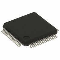
STM32F103RDT6 STMicroelectronics, STM32F103RDT6 Datasheet - Page 88

STM32F103RDT6
Manufacturer Part Number
STM32F103RDT6
Description
MCU ARM 32BIT 384KB FLASH 64LQFP
Manufacturer
STMicroelectronics
Series
STM32r
Specifications of STM32F103RDT6
Core Processor
ARM® Cortex-M3™
Core Size
32-Bit
Speed
72MHz
Connectivity
CAN, I²C, IrDA, LIN, SPI, UART/USART, USB
Peripherals
DMA, Motor Control PWM, PDR, POR, PVD, PWM, Temp Sensor, WDT
Number Of I /o
51
Program Memory Size
384KB (384K x 8)
Program Memory Type
FLASH
Ram Size
64K x 8
Voltage - Supply (vcc/vdd)
2 V ~ 3.6 V
Data Converters
A/D 16x12b; D/A 2x12b
Oscillator Type
Internal
Operating Temperature
-40°C ~ 85°C
Package / Case
64-LQFP
Processor Series
STM32F103x
Core
ARM Cortex M3
Data Bus Width
32 bit
Data Ram Size
64 KB
Interface Type
CAN, I2C, SPI, USART
Maximum Clock Frequency
72 MHz
Number Of Programmable I/os
51
Number Of Timers
8
Maximum Operating Temperature
+ 85 C
Mounting Style
SMD/SMT
3rd Party Development Tools
EWARM, EWARM-BL, MDK-ARM, RL-ARM, ULINK2
Minimum Operating Temperature
- 40 C
On-chip Adc
3 (12 bit, 16 Channel)
On-chip Dac
2 (12 bit, 2 Channel)
Featured Product
STM32 Cortex-M3 Companion Products
Eeprom Size
-
Cpu Family
STM32
Device Core
ARM Cortex-M3
Device Core Size
32b
Frequency (max)
72MHz
Total Internal Ram Size
64KB
# I/os (max)
51
Number Of Timers - General Purpose
8
Operating Supply Voltage (typ)
2.5/3.3V
Operating Supply Voltage (max)
3.6V
Operating Supply Voltage (min)
2V
Instruction Set Architecture
RISC
Operating Temp Range
-40C to 85C
Operating Temperature Classification
Industrial
Mounting
Surface Mount
Pin Count
64
Package Type
LQFP
For Use With
497-10048 - BOARD EVAL ACCELEROMETER497-10030 - STARTER KIT FOR STM32KSDKSTM32-PL - KIT IAR KICKSTART STM32 CORTEXM3497-8512 - KIT STARTER FOR STM32F10XE MCU497-8511 - KIT STARTER FOR STM32 512K FLASH497-8505 - KIT STARTER FOR STM32F10XE MCU497-6438 - BOARD EVALUTION FOR STM32 512K497-6289 - KIT PERFORMANCE STICK FOR STM32MCBSTM32UME - BOARD EVAL MCBSTM32 + ULINK-MEMCBSTM32U - BOARD EVAL MCBSTM32 + ULINK2MCBSTM32 - BOARD EVAL FOR STM STM32X SER497-6053 - KIT STARTER FOR STM32497-6052 - KIT STARTER FOR STM32497-6050 - KIT STARTER FOR STM32497-6049 - KIT EVALUATION LOW COST STM32497-6048 - BOARD EVALUATION FOR STM32497-6047 - KIT DEVELOPMENT FOR STM32
Lead Free Status / RoHS Status
Lead free / RoHS Compliant
Eeprom Size
-
Lead Free Status / Rohs Status
Details
Available stocks
Company
Part Number
Manufacturer
Quantity
Price
Company:
Part Number:
STM32F103RDT6
Manufacturer:
STM
Quantity:
50
Company:
Part Number:
STM32F103RDT6
Manufacturer:
STMicroelectronics
Quantity:
1 100
Company:
Part Number:
STM32F103RDT6
Manufacturer:
STMicroelectronics
Quantity:
10 000
Part Number:
STM32F103RDT6
Manufacturer:
ST
Quantity:
20 000
Company:
Part Number:
STM32F103RDT6TR
Manufacturer:
STMicroelectronics
Quantity:
10 000
Electrical characteristics
5.3.16
88/123
Communications interfaces
I
Unless otherwise specified, the parameters given in
performed under ambient temperature, f
summarized in
The STM32F103xC, STM32F103xD and STM32F103xE performance line I
meets the requirements of the standard I
restrictions: the I/O pins SDA and SCL are mapped to are not “true” open-drain. When
configured as open-drain, the PMOS connected between the I/O pin and V
but is still present.
The I
characteristics
and SCL) .
Table 50.
1. Guaranteed by design, not tested in production.
2. f
3. The maximum hold time of the Start condition has only to be met if the interface does not stretch the low
4. The device must internally provide a hold time of at least 300ns for the SDA signal in order to bridge the
2
t
C interface characteristics
w(STO:STA)
Symbol
t
t
t
t
t
w(SCLH)
w(SCLL)
t
su(SDA)
t
t
su(STO)
higher than 4 MHz to achieve the maximum fast mode I
period of SCL signal.
undefined region of the falling edge of SCL.
t
t
t
su(STA)
h(SDA)
PCLK1
r(SDA)
h(STA)
r(SCL)
f(SDA)
f(SCL)
C
2
C characteristics are described in
b
must be higher than 2 MHz to achieve the maximum standard mode I
SCL clock low time
SCL clock high time
SDA setup time
SDA data hold time
SDA and SCL rise time
SDA and SCL fall time
Start condition hold time
Repeated Start condition
setup time
Stop condition setup time
Stop to Start condition time
(bus free)
Capacitive load for each bus
line
I
2
C characteristics
for more details on the input/output alternate function characteristics (SDA
Table
Parameter
10.
Doc ID 14611 Rev 7
Standard mode I
PCLK1
Table
2
C communication protocol with the following
Min
250
0
STM32F103xC, STM32F103xD, STM32F103xE
4.7
4.0
4.0
4.7
4.0
4.7
(3)
frequency and V
50. Refer also to
2
C frequency.
Table 50
1000
Max
300
400
2
C
(1)
are derived from tests
20 + 0.1C
DD
Fast mode I
Section 5.3.13: I/O port
2
Min
100
C frequency. It must be
0
1.3
0.6
0.6
0.6
0.6
1.3
supply voltage conditions
(4)
b
DD
2
2
C
900
C interface
Max
300
300
400
(1)(2)
is disabled,
(3)
Unit
s
s
pF
µs
ns
µs


