MC908QY4ACDWE Freescale Semiconductor, MC908QY4ACDWE Datasheet - Page 130
MC908QY4ACDWE
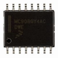
Manufacturer Part Number
MC908QY4ACDWE
Description
IC MCU 8BIT 4K FLASH 16-SOIC
Manufacturer
Freescale Semiconductor
Series
HC08r
Datasheet
1.MC908QT1ACDWE.pdf
(200 pages)
Specifications of MC908QY4ACDWE
Core Processor
HC08
Core Size
8-Bit
Speed
8MHz
Peripherals
LVD, POR, PWM
Number Of I /o
13
Program Memory Size
4KB (4K x 8)
Program Memory Type
FLASH
Ram Size
128 x 8
Voltage - Supply (vcc/vdd)
2.7 V ~ 5.5 V
Data Converters
A/D 6x10b
Oscillator Type
Internal
Operating Temperature
-40°C ~ 85°C
Package / Case
16-SOIC (0.300", 7.5mm Width)
Processor Series
HC08QY
Core
HC08
Data Bus Width
8 bit
Data Ram Size
128 B
Maximum Clock Frequency
8 MHz
Number Of Programmable I/os
13
Number Of Timers
2
Maximum Operating Temperature
+ 85 C
Mounting Style
SMD/SMT
Development Tools By Supplier
FSICEBASE, M68CBL05AE, DEMO908QB8, DEMO908QC16
Minimum Operating Temperature
- 40 C
On-chip Adc
10 bit, 6 Channel
Lead Free Status / RoHS Status
Lead free / RoHS Compliant
Eeprom Size
-
Connectivity
-
Lead Free Status / Rohs Status
Details
Available stocks
Company
Part Number
Manufacturer
Quantity
Price

Part Number:
MC908QY4ACDWE
Manufacturer:
FREESCALE
Quantity:
20 000
Part Number:
MC908QY4ACDWER
Manufacturer:
FREESCALE
Quantity:
20 000


Timer Interface Module (TIM)
14.3.4.3 PWM Initialization
To ensure correct operation when generating unbuffered or buffered PWM signals, use the following
initialization procedure:
Setting MS0B links channels 0 and 1 and configures them for buffered PWM operation. The TIM
channel 0 registers (TCH0H:TCH0L) initially control the buffered PWM output. TIM status control register
0 (TSCR0) controls and monitors the PWM signal from the linked channels. MS0B takes priority over
MS0A.
Clearing the toggle-on-overflow bit, TOVx, inhibits output toggles on TIM overflows. Subsequent output
compares try to force the output to a state it is already in and have no effect. The result is a 0% duty cycle
output.
Setting the channel x maximum duty cycle bit (CHxMAX) and setting the TOVx bit generates a 100% duty
cycle output. See
130
1. In the TIM status and control register (TSC):
2. In the TIM counter modulo registers (TMODH:TMODL), write the value for the required PWM
3. In the TIM channel x registers (TCHxH:TCHxL), write the value for the required pulse width.
4. In TIM channel x status and control register (TSCx):
5. In the TIM status control register (TSC), clear the TIM stop bit, TSTOP.
period.
a. Stop the counter by setting the TIM stop bit, TSTOP.
b. Reset the counter and prescaler by setting the TIM reset bit, TRST.
a. Write 0:1 (for unbuffered output compare or PWM signals) or 1:0 (for buffered output compare
b. Write 1 to the toggle-on-overflow bit, TOVx.
c. Write 1:0 (polarity 1 — to clear output on compare) or 1:1 (polarity 0 — to set output on
or PWM signals) to the mode select bits, MSxB:MSxA. See
compare) to the edge/level select bits, ELSxB:ELSxA. The output action on compare must
force the output to the complement of the pulse width level. See
channel. Writing to the active channel registers is the same as generating
unbuffered PWM signals.
In PWM signal generation, do not program the PWM channel to toggle on
output compare. Toggling on output compare prevents reliable 0% duty
cycle generation and removes the ability of the channel to self-correct in the
event of software error or noise. Toggling on output compare can also
cause incorrect PWM signal generation when changing the PWM pulse
width to a new, much larger value.
14.8.1 TIM Status and Control
MC68HC908QYA/QTA Family Data Sheet, Rev. 3
NOTE
Register.
Table
Table
14-2.
14-2.
Freescale Semiconductor
Related parts for MC908QY4ACDWE
Image
Part Number
Description
Manufacturer
Datasheet
Request
R

Part Number:
Description:
Manufacturer:
Freescale Semiconductor, Inc
Datasheet:
Part Number:
Description:
Manufacturer:
Freescale Semiconductor, Inc
Datasheet:
Part Number:
Description:
Manufacturer:
Freescale Semiconductor, Inc
Datasheet:
Part Number:
Description:
Manufacturer:
Freescale Semiconductor, Inc
Datasheet:
Part Number:
Description:
Manufacturer:
Freescale Semiconductor, Inc
Datasheet:
Part Number:
Description:
Manufacturer:
Freescale Semiconductor, Inc
Datasheet:
Part Number:
Description:
Manufacturer:
Freescale Semiconductor, Inc
Datasheet:
Part Number:
Description:
Manufacturer:
Freescale Semiconductor, Inc
Datasheet:
Part Number:
Description:
Manufacturer:
Freescale Semiconductor, Inc
Datasheet:
Part Number:
Description:
Manufacturer:
Freescale Semiconductor, Inc
Datasheet:
Part Number:
Description:
Manufacturer:
Freescale Semiconductor, Inc
Datasheet:
Part Number:
Description:
Manufacturer:
Freescale Semiconductor, Inc
Datasheet:
Part Number:
Description:
Manufacturer:
Freescale Semiconductor, Inc
Datasheet:
Part Number:
Description:
Manufacturer:
Freescale Semiconductor, Inc
Datasheet:
Part Number:
Description:
Manufacturer:
Freescale Semiconductor, Inc
Datasheet: