MC908QY4ACDWE Freescale Semiconductor, MC908QY4ACDWE Datasheet - Page 135
MC908QY4ACDWE
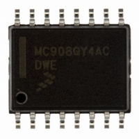
Manufacturer Part Number
MC908QY4ACDWE
Description
IC MCU 8BIT 4K FLASH 16-SOIC
Manufacturer
Freescale Semiconductor
Series
HC08r
Datasheet
1.MC908QT1ACDWE.pdf
(200 pages)
Specifications of MC908QY4ACDWE
Core Processor
HC08
Core Size
8-Bit
Speed
8MHz
Peripherals
LVD, POR, PWM
Number Of I /o
13
Program Memory Size
4KB (4K x 8)
Program Memory Type
FLASH
Ram Size
128 x 8
Voltage - Supply (vcc/vdd)
2.7 V ~ 5.5 V
Data Converters
A/D 6x10b
Oscillator Type
Internal
Operating Temperature
-40°C ~ 85°C
Package / Case
16-SOIC (0.300", 7.5mm Width)
Processor Series
HC08QY
Core
HC08
Data Bus Width
8 bit
Data Ram Size
128 B
Maximum Clock Frequency
8 MHz
Number Of Programmable I/os
13
Number Of Timers
2
Maximum Operating Temperature
+ 85 C
Mounting Style
SMD/SMT
Development Tools By Supplier
FSICEBASE, M68CBL05AE, DEMO908QB8, DEMO908QC16
Minimum Operating Temperature
- 40 C
On-chip Adc
10 bit, 6 Channel
Lead Free Status / RoHS Status
Lead free / RoHS Compliant
Eeprom Size
-
Connectivity
-
Lead Free Status / Rohs Status
Details
Available stocks
Company
Part Number
Manufacturer
Quantity
Price

Part Number:
MC908QY4ACDWE
Manufacturer:
FREESCALE
Quantity:
20 000
Part Number:
MC908QY4ACDWER
Manufacturer:
FREESCALE
Quantity:
20 000


14.8.4 TIM Channel Status and Control Registers
Each of the TIM channel status and control registers does the following:
CHxF — Channel x Flag Bit
CHxIE — Channel x Interrupt Enable Bit
MSxB — Mode Select Bit B
Freescale Semiconductor
•
•
•
•
•
•
•
•
When channel x is an input capture channel, this read/write bit is set when an active edge occurs on
the channel x pin. When channel x is an output compare channel, CHxF is set when the value in the
counter registers matches the value in the TIM channel x registers.
Clear CHxF by reading the TSCx register with CHxF set and then writing a 0 to CHxF. If another
interrupt request occurs before the clearing sequence is complete, then writing 0 to CHxF has no
effect. Therefore, an interrupt request cannot be lost due to inadvertent clearing of CHxF.
Writing a 1 to CHxF has no effect.
This read/write bit enables TIM interrupt service requests on channel x.
This read/write bit selects buffered output compare/PWM operation. MSxB exists only in the TSC0.
1 = Input capture or output compare on channel x
0 = No input capture or output compare on channel x
1 = Channel x interrupt requests enabled
0 = Channel x interrupt requests disabled
Flags input captures and output compares
Enables input capture and output compare interrupts
Selects input capture, output compare, or PWM operation
Selects high, low, or toggling output on output compare
Selects rising edge, falling edge, or any edge as the active input capture trigger
Selects output toggling on TIM overflow
Selects 0% and 100% PWM duty cycle
Selects buffered or unbuffered output compare/PWM operation
Reset:
Reset:
Read:
Write:
Read:
Write:
Figure 14-10. TIM Channel 1 Status and Control Register (TSC1)
Figure 14-9. TIM Channel 0 Status and Control Register (TSC0)
CH0F
CH1F
Bit 7
Bit 7
0
0
0
0
= Unimplemented
CH0IE
CH1IE
MC68HC908QYA/QTA Family Data Sheet, Rev. 3
6
0
6
0
MS0B
5
0
5
0
0
MS0A
MS1A
0
0
4
4
ELS0B
ELS1B
3
0
3
0
ELS0A
ELS1A
2
0
2
0
TOV0
TOV1
1
0
1
0
CH0MAX
CH1MAX
Bit 0
Bit 0
0
0
Registers
135
Related parts for MC908QY4ACDWE
Image
Part Number
Description
Manufacturer
Datasheet
Request
R

Part Number:
Description:
Manufacturer:
Freescale Semiconductor, Inc
Datasheet:
Part Number:
Description:
Manufacturer:
Freescale Semiconductor, Inc
Datasheet:
Part Number:
Description:
Manufacturer:
Freescale Semiconductor, Inc
Datasheet:
Part Number:
Description:
Manufacturer:
Freescale Semiconductor, Inc
Datasheet:
Part Number:
Description:
Manufacturer:
Freescale Semiconductor, Inc
Datasheet:
Part Number:
Description:
Manufacturer:
Freescale Semiconductor, Inc
Datasheet:
Part Number:
Description:
Manufacturer:
Freescale Semiconductor, Inc
Datasheet:
Part Number:
Description:
Manufacturer:
Freescale Semiconductor, Inc
Datasheet:
Part Number:
Description:
Manufacturer:
Freescale Semiconductor, Inc
Datasheet:
Part Number:
Description:
Manufacturer:
Freescale Semiconductor, Inc
Datasheet:
Part Number:
Description:
Manufacturer:
Freescale Semiconductor, Inc
Datasheet:
Part Number:
Description:
Manufacturer:
Freescale Semiconductor, Inc
Datasheet:
Part Number:
Description:
Manufacturer:
Freescale Semiconductor, Inc
Datasheet:
Part Number:
Description:
Manufacturer:
Freescale Semiconductor, Inc
Datasheet:
Part Number:
Description:
Manufacturer:
Freescale Semiconductor, Inc
Datasheet: