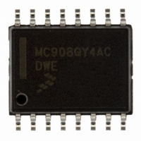
MC908QY4ACDWE Freescale Semiconductor, MC908QY4ACDWE Datasheet - Page 192

MC908QY4ACDWE
Manufacturer Part Number
MC908QY4ACDWE
Description
IC MCU 8BIT 4K FLASH 16-SOIC
Manufacturer
Freescale Semiconductor
Series
HC08r
Datasheet
1.MC908QT1ACDWE.pdf
(200 pages)
Specifications of MC908QY4ACDWE
Core Processor
HC08
Core Size
8-Bit
Speed
8MHz
Peripherals
LVD, POR, PWM
Number Of I /o
13
Program Memory Size
4KB (4K x 8)
Program Memory Type
FLASH
Ram Size
128 x 8
Voltage - Supply (vcc/vdd)
2.7 V ~ 5.5 V
Data Converters
A/D 6x10b
Oscillator Type
Internal
Operating Temperature
-40°C ~ 85°C
Package / Case
16-SOIC (0.300", 7.5mm Width)
Processor Series
HC08QY
Core
HC08
Data Bus Width
8 bit
Data Ram Size
128 B
Maximum Clock Frequency
8 MHz
Number Of Programmable I/os
13
Number Of Timers
2
Maximum Operating Temperature
+ 85 C
Mounting Style
SMD/SMT
Development Tools By Supplier
FSICEBASE, M68CBL05AE, DEMO908QB8, DEMO908QC16
Minimum Operating Temperature
- 40 C
On-chip Adc
10 bit, 6 Channel
Lead Free Status / RoHS Status
Lead free / RoHS Compliant
Eeprom Size
-
Connectivity
-
Lead Free Status / Rohs Status
Details
Available stocks
Company
Part Number
Manufacturer
Quantity
Price
Part Number:
MC908QY4ACDWE
Manufacturer:
FREESCALE
Quantity:
20 000
Part Number:
MC908QY4ACDWER
Manufacturer:
FREESCALE
Quantity:
20 000
A.2.1.1 Registers Affected
The ADCHx bits can be used to select additional ADC channels or bandgap measurement.
10-bit ADC uses the new ADRH register for the upper 2 bits.
A long sample time option has been added to conserve power at the expense of longer conversion times.
This option is selected using the new ADLSMP bit in the ADCLK register. (The bit location was previously
reserved.)
The ADC will now run in stop mode if the ACLKEN bit is set to enable the asynchronous clock inside the
ADC module. Utilizing stop mode for an ADC conversion gives the quietest operating mode to get
extremely accurate ADC readings. (This bit location now used by ACLKEN was reserved — it always read
as a 0 and writes to that location had no affect.)
192
•
•
•
The ADC that is on the QYxA can operate while the MCU is in stop mode allowing lower power
operation. This also adds a lower noise environment for precise ADC results.
Enabling an ADC channel no longer overrides the digital I/O function of the associated pin. To
prevent the digital I/O from interfering with the ADC read of the pin, the data direction bit associated
with the port pin must be set as input.
Finally, the new ADC can be configured to select two different reference clock sources:
–
–
The internal asynchronous clock source allows the ADC to be clocked for operation in stop mode.
The internal bus x 4
An internal asynchronous source
Reset:
Reset:
Reset:
Read:
Read:
Read:
Write:
Write:
Write:
Figure A-2. ADC10 Data Register High (ADRH), 10-Bit Mode
Figure A-1. ADC10 Status and Control Register (ADSCR)
ADLPC
COCO
Bit 7
Bit 7
Bit 7
0
0
0
0
Figure A-3. ADC10 Clock Register (ADCLK)
= Unimplemented
= Unimplemented
ADIV1
MC68HC908QYA/QTA Family Data Sheet, Rev. 3
AIEN
0
0
6
0
6
0
6
ADCO
ADIV0
5
0
5
0
0
5
0
ADICLK
ADCH4
4
1
4
0
0
4
0
MODE1
ADCH3
3
1
3
0
0
3
0
MODE0
ADCH2
2
1
2
0
0
2
0
ADLSMP
ADCH1
AD9
1
1
1
0
1
0
Freescale Semiconductor
ACLKEN
ADCH0
Bit 0
Bit 0
AD8
Bit 0
1
0
0


