MC908QY4ACDWE Freescale Semiconductor, MC908QY4ACDWE Datasheet - Page 29
MC908QY4ACDWE
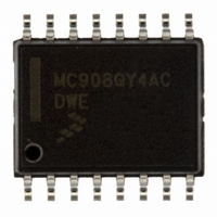
Manufacturer Part Number
MC908QY4ACDWE
Description
IC MCU 8BIT 4K FLASH 16-SOIC
Manufacturer
Freescale Semiconductor
Series
HC08r
Datasheet
1.MC908QT1ACDWE.pdf
(200 pages)
Specifications of MC908QY4ACDWE
Core Processor
HC08
Core Size
8-Bit
Speed
8MHz
Peripherals
LVD, POR, PWM
Number Of I /o
13
Program Memory Size
4KB (4K x 8)
Program Memory Type
FLASH
Ram Size
128 x 8
Voltage - Supply (vcc/vdd)
2.7 V ~ 5.5 V
Data Converters
A/D 6x10b
Oscillator Type
Internal
Operating Temperature
-40°C ~ 85°C
Package / Case
16-SOIC (0.300", 7.5mm Width)
Processor Series
HC08QY
Core
HC08
Data Bus Width
8 bit
Data Ram Size
128 B
Maximum Clock Frequency
8 MHz
Number Of Programmable I/os
13
Number Of Timers
2
Maximum Operating Temperature
+ 85 C
Mounting Style
SMD/SMT
Development Tools By Supplier
FSICEBASE, M68CBL05AE, DEMO908QB8, DEMO908QC16
Minimum Operating Temperature
- 40 C
On-chip Adc
10 bit, 6 Channel
Lead Free Status / RoHS Status
Lead free / RoHS Compliant
Eeprom Size
-
Connectivity
-
Lead Free Status / Rohs Status
Details
Available stocks
Company
Part Number
Manufacturer
Quantity
Price

Part Number:
MC908QY4ACDWE
Manufacturer:
FREESCALE
Quantity:
20 000
Part Number:
MC908QY4ACDWER
Manufacturer:
FREESCALE
Quantity:
20 000


2.6 FLASH Memory (FLASH)
The FLASH memory is intended primarily for program storage. In-circuit programming allows the
operating program to be loaded into the FLASH memory after final assembly of the application product.
It is possible to program the entire array through the single-wire monitor mode interface. Because no
special voltages are needed for FLASH erase and programming operations, in-application programming
is also possible through other software-controlled communication paths.
This subsection describes the operation of the embedded FLASH memory. The FLASH memory can be
read, programmed, and erased from the internal V
enabled through the use of an internal charge pump.
The minimum size of FLASH memory that can be erased is 64 bytes; and the maximum size of FLASH
memory that can be programmed in a program cycle is 32 bytes (a row). Program and erase operations
are facilitated through control bits in the FLASH control register (FLCR). Details for these operations
appear later in this section.
2.6.1 FLASH Control Register
The FLASH control register (FLCR) controls FLASH program and erase operations.
HVEN — High Voltage Enable Bit
MASS — Mass Erase Control Bit
Freescale Semiconductor
1. No security feature is absolutely secure. However, Freescale’s strategy is to make reading or copying the FLASH difficult
This read/write bit enables high voltage from the charge pump to the memory for either program or
erase operation. It can only be set if either PGM =1 or ERASE =1 and the proper sequence for
program or erase is followed.
This read/write bit configures the memory for mass erase operation.
for unauthorized users.
1 = High voltage enabled to array and charge pump on
0 = High voltage disabled to array and charge pump off
1 = Mass erase operation selected
0 = Mass erase operation unselected
Reset:
Read:
Write:
An erased bit reads as a 1 and a programmed bit reads as a 0. A security
feature prevents viewing of the FLASH contents.
Bit 7
0
0
= Unimplemented
Figure 2-3. FLASH Control Register (FLCR)
MC68HC908QYA/QTA Family Data Sheet, Rev. 3
6
0
0
5
0
0
NOTE
4
0
0
DD
supply. The program and erase operations are
HVEN
3
0
(1)
MASS
2
0
ERASE
1
0
FLASH Memory (FLASH)
PGM
Bit 0
0
29
Related parts for MC908QY4ACDWE
Image
Part Number
Description
Manufacturer
Datasheet
Request
R

Part Number:
Description:
Manufacturer:
Freescale Semiconductor, Inc
Datasheet:
Part Number:
Description:
Manufacturer:
Freescale Semiconductor, Inc
Datasheet:
Part Number:
Description:
Manufacturer:
Freescale Semiconductor, Inc
Datasheet:
Part Number:
Description:
Manufacturer:
Freescale Semiconductor, Inc
Datasheet:
Part Number:
Description:
Manufacturer:
Freescale Semiconductor, Inc
Datasheet:
Part Number:
Description:
Manufacturer:
Freescale Semiconductor, Inc
Datasheet:
Part Number:
Description:
Manufacturer:
Freescale Semiconductor, Inc
Datasheet:
Part Number:
Description:
Manufacturer:
Freescale Semiconductor, Inc
Datasheet:
Part Number:
Description:
Manufacturer:
Freescale Semiconductor, Inc
Datasheet:
Part Number:
Description:
Manufacturer:
Freescale Semiconductor, Inc
Datasheet:
Part Number:
Description:
Manufacturer:
Freescale Semiconductor, Inc
Datasheet:
Part Number:
Description:
Manufacturer:
Freescale Semiconductor, Inc
Datasheet:
Part Number:
Description:
Manufacturer:
Freescale Semiconductor, Inc
Datasheet:
Part Number:
Description:
Manufacturer:
Freescale Semiconductor, Inc
Datasheet:
Part Number:
Description:
Manufacturer:
Freescale Semiconductor, Inc
Datasheet: