MC908QY4ACDWE Freescale Semiconductor, MC908QY4ACDWE Datasheet - Page 73
MC908QY4ACDWE
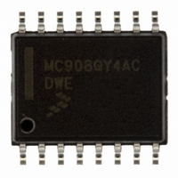
Manufacturer Part Number
MC908QY4ACDWE
Description
IC MCU 8BIT 4K FLASH 16-SOIC
Manufacturer
Freescale Semiconductor
Series
HC08r
Datasheet
1.MC908QT1ACDWE.pdf
(200 pages)
Specifications of MC908QY4ACDWE
Core Processor
HC08
Core Size
8-Bit
Speed
8MHz
Peripherals
LVD, POR, PWM
Number Of I /o
13
Program Memory Size
4KB (4K x 8)
Program Memory Type
FLASH
Ram Size
128 x 8
Voltage - Supply (vcc/vdd)
2.7 V ~ 5.5 V
Data Converters
A/D 6x10b
Oscillator Type
Internal
Operating Temperature
-40°C ~ 85°C
Package / Case
16-SOIC (0.300", 7.5mm Width)
Processor Series
HC08QY
Core
HC08
Data Bus Width
8 bit
Data Ram Size
128 B
Maximum Clock Frequency
8 MHz
Number Of Programmable I/os
13
Number Of Timers
2
Maximum Operating Temperature
+ 85 C
Mounting Style
SMD/SMT
Development Tools By Supplier
FSICEBASE, M68CBL05AE, DEMO908QB8, DEMO908QC16
Minimum Operating Temperature
- 40 C
On-chip Adc
10 bit, 6 Channel
Lead Free Status / RoHS Status
Lead free / RoHS Compliant
Eeprom Size
-
Connectivity
-
Lead Free Status / Rohs Status
Details
Available stocks
Company
Part Number
Manufacturer
Quantity
Price

Part Number:
MC908QY4ACDWE
Manufacturer:
FREESCALE
Quantity:
20 000
Part Number:
MC908QY4ACDWER
Manufacturer:
FREESCALE
Quantity:
20 000


Freescale Semiconductor
JMP opr
JMP opr
JMP opr,X
JMP opr,X
JMP ,X
JSR opr
JSR opr
JSR opr,X
JSR opr,X
JSR ,X
LDA #opr
LDA opr
LDA opr
LDA opr,X
LDA opr,X
LDA ,X
LDA opr,SP
LDA opr,SP
LDHX #opr
LDHX opr
LDX #opr
LDX opr
LDX opr
LDX opr,X
LDX opr,X
LDX ,X
LDX opr,SP
LDX opr,SP
LSL opr
LSLA
LSLX
LSL opr,X
LSL ,X
LSL opr,SP
LSR opr
LSRA
LSRX
LSR opr,X
LSR ,X
LSR opr,SP
MOV opr,opr
MOV opr,X+
MOV #opr,opr
MOV X+,opr
MUL
NEG opr
NEGA
NEGX
NEG opr,X
NEG ,X
NEG opr,SP
NOP
NSA
ORA #opr
ORA opr
ORA opr
ORA opr,X
ORA opr,X
ORA ,X
ORA opr,SP
ORA opr,SP
PSHA
PSHH
PSHX
Source
Form
Jump to Subroutine
Load A from M
Load H:X from M
Load X from M
Logical Shift Left
(Same as ASL)
Logical Shift Right
Move
Unsigned multiply
Negate (Two’s Complement)
No Operation
Nibble Swap A
Inclusive OR A and M
Push A onto Stack
Push H onto Stack
Push X onto Stack
Jump
Operation
Table 7-1. Instruction Set Summary (Sheet 4 of 6)
MC68HC908QYA/QTA Family Data Sheet, Rev. 3
PC ← (PC) + n (n = 1, 2, or 3)
H:X ← (H:X) + 1 (IX+D, DIX+)
PC ← Unconditional Address
Push (PCH); SP ← (SP) – 1
Push (PCL); SP ← (SP) – 1
0
C
(M)
Push (H); SP ← (SP) – 1
Push (A); SP ← (SP) – 1
Push (X); SP ← (SP) – 1
M ← –(M) = $00 – (M)
M ← –(M) = $00 – (M)
M ← –(M) = $00 – (M)
PC ← Jump Address
A ← –(A) = $00 – (A)
X ← –(X) = $00 – (X)
A ← (A[3:0]:A[7:4])
Destination
b7
H:X ← (M:M + 1)
b7
X:A ← (X) × (A)
Description
A ← (A) | (M)
A ← (M)
X ← (M)
None
← (M)
b0
b0
Source
C
0
V H I N Z C
– – – – – –
– – – – – –
0 – –
0 – –
0 – –
0 – –
– 0 – – – 0 INH
– – – – – – INH
– – – – – – INH
0 – –
– – – – – – INH
– – – – – – INH
– – – – – – INH
– –
– – 0
– –
on CCR
Effect
Instruction Set Summary
–
–
–
–
–
DIR
EXT
IX2
IX1
IX
DIR
EXT
IX2
IX1
IX
IMM
DIR
EXT
IX2
IX1
IX
SP1
SP2
IMM
DIR
IMM
DIR
EXT
IX2
IX1
IX
SP1
SP2
DIR
INH
INH
IX1
IX
SP1
DIR
INH
INH
IX1
IX
SP1
DD
DIX+
IMD
IX+D
DIR
INH
INH
IX1
IX
SP1
IMM
DIR
EXT
IX2
IX1
IX
SP1
SP2
9EDE
9EE6
9ED6
9EEE
9EEA
9EDA
9E68
9E64
9E60
CC
DC
CD
DD
BC
EC
FC
BD
ED
FD
C6
D6
AE
BE
CE
DE
EE
FE
9D
AA
BA
CA
DA
EA
A6
B6
E6
F6
45
55
38
48
58
68
78
34
44
54
64
74
4E
5E
6E
7E
42
30
40
50
60
70
62
FA
87
8B
89
dd
hh ll
ee ff
ff
dd
hh ll
ee ff
ff
ii
dd
hh ll
ee ff
ff
ff
ee ff
ii jj
dd
ii
dd
hh ll
ee ff
ff
ff
ee ff
dd
ff
ff
dd
ff
ff
dd dd
dd
ii dd
dd
dd
ff
ff
ii
dd
hh ll
ee ff
ff
ff
ee ff
73
2
3
4
3
2
4
5
6
5
4
2
3
4
4
3
2
4
5
3
4
2
3
4
4
3
2
4
5
4
1
1
4
3
5
4
1
1
4
3
5
5
4
4
4
5
4
1
1
4
3
5
1
3
2
3
4
4
3
2
4
5
2
2
2
Related parts for MC908QY4ACDWE
Image
Part Number
Description
Manufacturer
Datasheet
Request
R

Part Number:
Description:
Manufacturer:
Freescale Semiconductor, Inc
Datasheet:
Part Number:
Description:
Manufacturer:
Freescale Semiconductor, Inc
Datasheet:
Part Number:
Description:
Manufacturer:
Freescale Semiconductor, Inc
Datasheet:
Part Number:
Description:
Manufacturer:
Freescale Semiconductor, Inc
Datasheet:
Part Number:
Description:
Manufacturer:
Freescale Semiconductor, Inc
Datasheet:
Part Number:
Description:
Manufacturer:
Freescale Semiconductor, Inc
Datasheet:
Part Number:
Description:
Manufacturer:
Freescale Semiconductor, Inc
Datasheet:
Part Number:
Description:
Manufacturer:
Freescale Semiconductor, Inc
Datasheet:
Part Number:
Description:
Manufacturer:
Freescale Semiconductor, Inc
Datasheet:
Part Number:
Description:
Manufacturer:
Freescale Semiconductor, Inc
Datasheet:
Part Number:
Description:
Manufacturer:
Freescale Semiconductor, Inc
Datasheet:
Part Number:
Description:
Manufacturer:
Freescale Semiconductor, Inc
Datasheet:
Part Number:
Description:
Manufacturer:
Freescale Semiconductor, Inc
Datasheet:
Part Number:
Description:
Manufacturer:
Freescale Semiconductor, Inc
Datasheet:
Part Number:
Description:
Manufacturer:
Freescale Semiconductor, Inc
Datasheet: