MC908QY4ACDWE Freescale Semiconductor, MC908QY4ACDWE Datasheet - Page 90
MC908QY4ACDWE
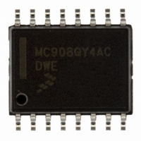
Manufacturer Part Number
MC908QY4ACDWE
Description
IC MCU 8BIT 4K FLASH 16-SOIC
Manufacturer
Freescale Semiconductor
Series
HC08r
Datasheet
1.MC908QT1ACDWE.pdf
(200 pages)
Specifications of MC908QY4ACDWE
Core Processor
HC08
Core Size
8-Bit
Speed
8MHz
Peripherals
LVD, POR, PWM
Number Of I /o
13
Program Memory Size
4KB (4K x 8)
Program Memory Type
FLASH
Ram Size
128 x 8
Voltage - Supply (vcc/vdd)
2.7 V ~ 5.5 V
Data Converters
A/D 6x10b
Oscillator Type
Internal
Operating Temperature
-40°C ~ 85°C
Package / Case
16-SOIC (0.300", 7.5mm Width)
Processor Series
HC08QY
Core
HC08
Data Bus Width
8 bit
Data Ram Size
128 B
Maximum Clock Frequency
8 MHz
Number Of Programmable I/os
13
Number Of Timers
2
Maximum Operating Temperature
+ 85 C
Mounting Style
SMD/SMT
Development Tools By Supplier
FSICEBASE, M68CBL05AE, DEMO908QB8, DEMO908QC16
Minimum Operating Temperature
- 40 C
On-chip Adc
10 bit, 6 Channel
Lead Free Status / RoHS Status
Lead free / RoHS Compliant
Eeprom Size
-
Connectivity
-
Lead Free Status / Rohs Status
Details
Available stocks
Company
Part Number
Manufacturer
Quantity
Price

Part Number:
MC908QY4ACDWE
Manufacturer:
FREESCALE
Quantity:
20 000
Part Number:
MC908QY4ACDWER
Manufacturer:
FREESCALE
Quantity:
20 000


Low-Voltage Inhibit (LVI)
The LVI module contains a bandgap reference circuit and comparator. When the LVITRIP bit is cleared,
the default state at power-on reset, V
trip points are specified in
Characteristics.
Because the default LVI trip point after power-on reset is configured for low voltage operation, a system
requiring high voltage LVI operation must set the LVITRIP bit during system initialization. V
above the LVI trip rising voltage, V
go into LVI reset.
After an LVI reset occurs, the MCU remains in reset until V
Integration Module (SIM)
The output of the comparator controls the state of the LVIOUT flag in the LVI status register (LVISR) and
can be used for polling LVI operation when the LVI reset is disabled.
The LVI is enabled out of reset. The following bits located in the configuration register can alter the default
conditions.
10.3.1 Polled LVI Operation
In applications that can operate at V
the LVIOUT bit. In the configuration register, LVIPWRD must be cleared to enable the LVI module, and
LVIRSTD must be set to disable LVI resets.
10.3.2 Forced Reset Operation
In applications that require V
module to reset the MCU when V
and LVIRSTD must be cleared to enable the LVI module and to enable LVI resets.
10.3.3 LVI Hysteresis
The LVI has hysteresis to maintain a stable operating condition. After the LVI has triggered (by having
V
V
approximately equal to V
10.3.4 LVI Trip Selection
LVITRIP in the configuration register selects the LVI protection range. The default setting out of reset is
for the low voltage range. Because LVITRIP is in a write-once configuration register, the protection range
cannot be changed after initialization.
90
DD
TRIPR
•
•
•
•
fall below V
Setting the LVI power disable bit, LVIPWRD, disables the LVI.
Setting the LVI reset disable bit, LVIRSTD, prevents the LVI module from generating a reset.
Setting the LVI enable in stop mode bit, LVISTOP, enables the LVI to operate in stop mode.
Setting the LVI trip point bit, LVITRIP, configures the trip point voltage (V
operating range.
. This prevents a condition in which the MCU is continually entering and exiting reset if V
The MCU is guaranteed to operate at a minimum supply voltage. The trip
point (V
section for the actual trip point voltages.
TRIPF
), the MCU will remain in reset until V
TRIPF
TRIPF
for the reset recovery sequence.
16.5 5-V DC Electrical Characteristics
) may be lower than this. See the Electrical Characteristics
DD
. V
MC68HC908QYA/QTA Family Data Sheet, Rev. 3
to remain above the V
TRIPR
DD
TRIPR
DD
falls below the V
TRIPF
levels below the V
is greater than V
, for the high voltage operating range or the MCU will immediately
is configured for the lower V
NOTE
TRIPF
TRIPF
TRIPF
TRIPF
DD
level. In the configuration register, LVIPWRD
DD
level, enabling LVI resets allows the LVI
rises above V
by the typical hysteresis voltage, V
rises above the rising trip point voltage,
level, software can monitor V
and
16.8 3-V DC Electrical
DD
TRIPR
operating range. The actual
TRIPF
. See
Freescale Semiconductor
) for the higher V
Chapter 13 System
DD
DD
must be
by polling
DD
HYS
is
.
DD
Related parts for MC908QY4ACDWE
Image
Part Number
Description
Manufacturer
Datasheet
Request
R

Part Number:
Description:
Manufacturer:
Freescale Semiconductor, Inc
Datasheet:
Part Number:
Description:
Manufacturer:
Freescale Semiconductor, Inc
Datasheet:
Part Number:
Description:
Manufacturer:
Freescale Semiconductor, Inc
Datasheet:
Part Number:
Description:
Manufacturer:
Freescale Semiconductor, Inc
Datasheet:
Part Number:
Description:
Manufacturer:
Freescale Semiconductor, Inc
Datasheet:
Part Number:
Description:
Manufacturer:
Freescale Semiconductor, Inc
Datasheet:
Part Number:
Description:
Manufacturer:
Freescale Semiconductor, Inc
Datasheet:
Part Number:
Description:
Manufacturer:
Freescale Semiconductor, Inc
Datasheet:
Part Number:
Description:
Manufacturer:
Freescale Semiconductor, Inc
Datasheet:
Part Number:
Description:
Manufacturer:
Freescale Semiconductor, Inc
Datasheet:
Part Number:
Description:
Manufacturer:
Freescale Semiconductor, Inc
Datasheet:
Part Number:
Description:
Manufacturer:
Freescale Semiconductor, Inc
Datasheet:
Part Number:
Description:
Manufacturer:
Freescale Semiconductor, Inc
Datasheet:
Part Number:
Description:
Manufacturer:
Freescale Semiconductor, Inc
Datasheet:
Part Number:
Description:
Manufacturer:
Freescale Semiconductor, Inc
Datasheet: