MC9S08QE8CLC Freescale Semiconductor, MC9S08QE8CLC Datasheet - Page 2
MC9S08QE8CLC
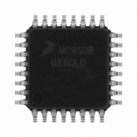
Manufacturer Part Number
MC9S08QE8CLC
Description
IC MCU 8BIT 8K FLASH 32-LQFP
Manufacturer
Freescale Semiconductor
Series
HCS08r
Specifications of MC9S08QE8CLC
Core Processor
HCS08
Core Size
8-Bit
Speed
20MHz
Connectivity
I²C, LIN, SCI, SPI
Peripherals
LVD, PWM, WDT
Number Of I /o
26
Program Memory Size
8KB (8K x 8)
Program Memory Type
FLASH
Ram Size
512 x 8
Voltage - Supply (vcc/vdd)
1.8 V ~ 3.6 V
Data Converters
A/D 10x12b
Oscillator Type
Internal
Operating Temperature
-40°C ~ 85°C
Package / Case
32-LQFP
Cpu Family
HCS08
Device Core Size
8b
Frequency (max)
20MHz
Interface Type
I2C/SCI/SPI
Total Internal Ram Size
512Byte
# I/os (max)
26
Number Of Timers - General Purpose
2
Operating Supply Voltage (typ)
2.5/3.3V
Operating Supply Voltage (max)
3.6V
Operating Supply Voltage (min)
1.8V
On-chip Adc
10-chx12-bit
Instruction Set Architecture
CISC
Operating Temp Range
-40C to 85C
Operating Temperature Classification
Industrial
Mounting
Surface Mount
Pin Count
32
Package Type
LQFP
Processor Series
S08QE
Core
HCS08
Data Bus Width
8 bit
Data Ram Size
512 B
Maximum Clock Frequency
20 MHz
Number Of Programmable I/os
26
Number Of Timers
2
Maximum Operating Temperature
+ 85 C
Mounting Style
SMD/SMT
3rd Party Development Tools
EWS08
Development Tools By Supplier
DEMOQE128, EVBQE128
Minimum Operating Temperature
- 40 C
Package
32LQFP
Family Name
HCS08
Maximum Speed
20 MHz
Operating Supply Voltage
2.5|3.3 V
For Use With
DEMO9S08QE8 - BOARD DEMO FOR MC9S08Q
Lead Free Status / RoHS Status
Lead free / RoHS Compliant
Eeprom Size
-
Lead Free Status / Rohs Status
Compliant
Available stocks
Company
Part Number
Manufacturer
Quantity
Price
Company:

Part Number:
MC9S08QE8CLC
Manufacturer:
QFP
Quantity:
648
Company:
Part Number:
MC9S08QE8CLC
Manufacturer:
Freescale Semiconductor
Quantity:
10 000


Freescale and the Freescale logo are trademarks or registered trademarks of Freescale Semiconductor, Inc. in the U.S. and other
countries. All other product or service names are the property of their respective owners.
© Freescale Semiconductor, Inc. 2009.
Document Number: QE84FS
REV 2
8-bit Fact Sheet
Features
Peripherals
Input/Output
• 27 General Purpose Input/Output (GPIO),
• 8 Keyboard Interrupts (KBI) pins with
System Protection
Development Support
• Analog-to-digital converter (ADC)—10-channel,
• Timer—two 3-channel (TPM1 and TPM2);
• Serial Communications Interface (SCI)—module
• Two analog comparators with option to compare
• Serial Peripheral Interface (SPI)—one module
• I
• Watchdog computer operating properly (COP)
• Low-voltage detection with reset or interrupt;
• Illegal op code and illegal address detection
• Flash block protection
• Single-wire background debug interface
• Breakpoint capability
• ICE debug module containing three comparators
one input-only and one output-only pin
selectable polarity
12-bit resolution; 2.5 µs conversion time; automatic
compare function; internal temperature sensor;
internal bandgap reference channel; operation
in stop mode
selectable input capture, output compare, or
buffered edge- or center-aligned PWM on each
channel
offering asynchronous communications,13-bit break
option, flexible baud rate generator, double buffered
transmit and receive and optional H/W parity
checking and generation
to an internal reference—output can be optionally
routed to timer/pulse width modulator (PWM) as
input capture trigger
with full-duplex or single-wire bidirectional;
double-buffered transmit and receive; master
or slave mode; MSB-first or LSB-first shifting
bus loading; multi-master operation; programmable
slave address; interrupt-driven byte-by-byte
data transfer; supports broadcast mode and
10-bit addressing
reset with option to run from dedicated 1 kHz
internal clock source or bus clock
selectable trip points
with reset
and nine trigger modes. Eight deep FIFO for
storing change-of-flow addresses and event-only
data—debug module supports both tag and
force breakpoints.
2
C with up to 100 kbps with maximum
Benefits
• Results in large number of flexible I/O pins that allow
• Can be used for reading input from a keypad or
• Having 10 channels allows up to 10 analog
• Accuracy and full functionality guaranteed across
• Two TPMs allow for two different time bases,
• Provides standard UART communications peripheral
• Allows full-duplex, asynchronous, NRZ serial
• Edge interrupt can wake up MCU from
• Requires only single pin for input signal, freeing
• Allows other components in system to see result
• Can be used for single slope ADC and RC time
• Allows high speed (up to 5 Mbps) communications
• I
• Allows device to recognize runaway code
• Alarms the developer of voltage drops outside
• Allows the device to recognize erroneous code
• Prevents unintentional programming of protected
• Allows developers to use the same hardware
• Allows single breakpoint setting during in-circuit
• Provides built-in full emulation without expense of
developers to easily interface device into their
own designs
used as general pin interrupts
devices to be sampled at extremely high speeds
1.8V to 3.6V operating voltage of the MCU
with a total of twelve timer channels
communication between MCU and remote devices
low-power mode
additional pins for other use
of comparator with minimal delay
constant measurements
to other MCUs or peripherals such as MC1319x
RF transceivers
using an additional I
an opportunity to add an additional I
(infinite loops) and resets processor to avoid
lock-up states
of the typical operating range
and resets the processor to avoid lock-up states
flash memory, which greatly reduces the chance of
losing vital system code for vendor applications
cables between S08 and V1 ColdFire
debugging (plus three more breakpoints in on-chip
debug module)
traditional emulator
2
C port enables increased system memory by
2
C EEPROM. This also creates
Learn More:
2
®
C device.
platforms
Cost-Effective Development Tools
DEMO9S08QE8
$69*
Cost-effective demonstration kit including the
QE8 daughter card, as well as serial port and
built-in USB-BDM cable for debugging and
programming. This tool includes a lab that
demonstrates the ultra-low-power benefits.
DC9S08QE8
$10*
Daughter card of QE8 to use on your
DEMOQE128 demonstration kit.
CodeWarrior
for Microcontrollers 6.1
Complimentary** Special Edition
CodeWarrior Development Studio for
Microcontrollers is a single tool suite
that supports software development for
Freescale’s 8- and 32-bit V1 ColdFire
microcontrollers. Designers can further
accelerate application development with the
help of Processor Expert™, an award-winning
rapid application development tool integrated
into the CodeWarrior tool suite.
* Prices indicated are MSRP
** Subject to license agreement
For more information about the
Flexis QE family, please visit
www.freescale.com/lowpower.
Package Options
Part Number
MC9S08QE4CPG
MC9S08QE4CTG
MC9S08QE4CWJ
MC9S08QE4CWL
MC9S08QE4CLC
MC9S08QE8CPG
MC9S08QE8CTG
MC9S08QE8CWJ
MC9S08QE8CWL
MC9S08QE8CLC
®
Development Studio
Temp. Range
-40°C to +85°C
-40°C to +85°C
-40°C to +85°C
-40°C to +85°C
-40°C to +85°C
-40°C to +85°C
-40°C to +85°C
-40°C to +85°C
-40°C to +85°C
-40°C to +85°C
Package
16-pin PDIP
16-pin TSSOP
20-pin SOIC
28-pin SOIC
32-pin LQFP
16-pin PDIP
16-pin TSSOP
20-pin SOIC
28-pin SOIC
32-pin LQFP
Related parts for MC9S08QE8CLC
Image
Part Number
Description
Manufacturer
Datasheet
Request
R

Part Number:
Description:
Manufacturer:
Freescale Semiconductor, Inc
Datasheet:
Part Number:
Description:
Manufacturer:
Freescale Semiconductor, Inc
Datasheet:
Part Number:
Description:
Manufacturer:
Freescale Semiconductor, Inc
Datasheet:
Part Number:
Description:
Manufacturer:
Freescale Semiconductor, Inc
Datasheet:
Part Number:
Description:
Manufacturer:
Freescale Semiconductor, Inc
Datasheet:
Part Number:
Description:
Manufacturer:
Freescale Semiconductor, Inc
Datasheet:
Part Number:
Description:
Manufacturer:
Freescale Semiconductor, Inc
Datasheet:
Part Number:
Description:
Manufacturer:
Freescale Semiconductor, Inc
Datasheet:
Part Number:
Description:
Manufacturer:
Freescale Semiconductor, Inc
Datasheet:
Part Number:
Description:
Manufacturer:
Freescale Semiconductor, Inc
Datasheet:
Part Number:
Description:
Manufacturer:
Freescale Semiconductor, Inc
Datasheet:
Part Number:
Description:
Manufacturer:
Freescale Semiconductor, Inc
Datasheet:
Part Number:
Description:
Manufacturer:
Freescale Semiconductor, Inc
Datasheet:
Part Number:
Description:
Manufacturer:
Freescale Semiconductor, Inc
Datasheet:
Part Number:
Description:
Manufacturer:
Freescale Semiconductor, Inc
Datasheet: