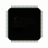
TMP86FS28DFG(JZ) Toshiba, TMP86FS28DFG(JZ) Datasheet - Page 168

TMP86FS28DFG(JZ)
Manufacturer Part Number
TMP86FS28DFG(JZ)
Description
IC MCU 8BIT FLASH 60KB 80-LQFP
Manufacturer
Toshiba
Series
TLCS-870/Cr
Datasheet
1.TMP86FS28DFGJZ.pdf
(272 pages)
Specifications of TMP86FS28DFG(JZ)
Core Processor
870/C
Core Size
8-Bit
Speed
16MHz
Connectivity
SIO, UART/USART
Peripherals
LCD, PWM, WDT
Number Of I /o
62
Program Memory Size
60KB (60K x 8)
Program Memory Type
FLASH
Ram Size
2K x 8
Voltage - Supply (vcc/vdd)
2.7 V ~ 5.5 V
Data Converters
A/D 8x10b
Oscillator Type
Internal
Operating Temperature
-40°C ~ 85°C
Package / Case
80-LQFP
Processor Series
TLCS-870
Core
870/C
Data Bus Width
8 bit
Data Ram Size
2 KB
Interface Type
SIO, UART
Maximum Clock Frequency
16 MHz
Number Of Programmable I/os
62
Number Of Timers
6
Maximum Operating Temperature
+ 85 C
Mounting Style
SMD/SMT
Development Tools By Supplier
BM1040R0A, BMP86A100010A, BMP86A100010B, BMP86A200010B, BMP86A200020A, BMP86A300010A, BMP86A300020A, BMP86A300030A, SW89CN0-ZCC, SW00MN0-ZCC
Minimum Operating Temperature
- 40 C
On-chip Adc
10 bit, 8 Channel
For Use With
BM1401W0A-G - FLASH WRITER ON-BOARD PROGRAMTMP89C900XBG - EMULATION CHIP TMP89F LQFP
Lead Free Status / RoHS Status
Lead free / RoHS Compliant
Eeprom Size
-
Lead Free Status / Rohs Status
Details
Other names
TMP86FS28DFGJZ
Available stocks
Company
Part Number
Manufacturer
Quantity
Price
- Current page: 168 of 272
- Download datasheet (3Mb)
11.6 Transfer Mode
11.6 Transfer Mode
11.6.1 4-bit and 8-bit transfer modes
SIOCR1<SIOM> is used to select the transmit, receive, or transmit/receive mode.
(number of transfer words to be transferred) to the data buffer registers (DBR).
output sequentially to the SO pin in synchronous with the serial clock, starting with the least significant bit
(LSB). As soon as the LSB has been output, the data are transferred from the data buffer register to the shift
register. When the final data bit has been transferred and the data buffer register is empty, an INTSIO (Buffer
empty) interrupt is generated to request the next transmitted data.
transmitted data are not loaded to the data buffer register by the time the number of data words specified with
the SIOCR2<BUF> has been transmitted. Writing even one word of data cancels the automatic-wait; therefore,
when transmitting two or more words, always write the next word before transmission of the previous word is
completed.
Thus, the transfer speed is determined by the maximum delay time from the generation of the interrupt request
to writing of the data to the data buffer register by the interrupt service program.
empty interrupt service program.
SCK pin
SO pin
INTSIO interrupt
SCK pin
SO pin
INTSIO interrupt
SCK pin
SI pin
INTSIO interrupt
In these modes, firstly set the SIO control register to the transmit mode, and then write first transmit data
When the internal clock is used, the serial clock will stop and an automatic-wait will be initiated if the next
Note:Automatic waits are also canceled by writing to a DBR not being used as a transmit data buffer register; there-
When an external clock is used, the data must be written to the data buffer register before shifting next data.
The transmission is ended by clearing SIOCR1<SIOS> to “0” or setting SIOCR1<SIOINH> to “1” in buffer
After the data are written, the transmission is started by setting SIOCR1<SIOS> to “1”. The data are then
Figure 11-6 Number of words to transfer (Example: 1word = 4bit)
fore, during SIO do not use such DBR for other applications. For example, when 3 words are transmitted, do
not use the DBR of the remained 5 words.
a
a
a
0
0
0
a
a
a
1
1
1
a
a
a
2
2
2
a
a
Page 156
3
3
(b) 3 words transmit
(a) 1 word transmit
(c) 3 words receive
b
b
0
0
a
3
b
b
1
1
b
b
2
2
b
b
3
3
c
c
0
0
c
c
1
1
c
c
2
2
c
c
3
3
TMP86FS28DFG
Related parts for TMP86FS28DFG(JZ)
Image
Part Number
Description
Manufacturer
Datasheet
Request
R
Part Number:
Description:
Toshiba Semiconductor [TOSHIBA IGBT Module Silicon N Channel IGBT]
Manufacturer:
TOSHIBA Semiconductor CORPORATION
Datasheet:
Part Number:
Description:
TOSHIBA GTR MODULE SILICON NPN TRIPLE DIFFUSED TYPE
Manufacturer:
TOSHIBA Semiconductor CORPORATION
Datasheet:
Part Number:
Description:
TOSHIBA GTR Module Silicon N Channel IGBT
Manufacturer:
TOSHIBA Semiconductor CORPORATION
Datasheet:
Part Number:
Description:
TOSHIBA Intelligent Power Module Silicon N Channel IGBT
Manufacturer:
TOSHIBA Semiconductor CORPORATION
Datasheet:
Part Number:
Description:
TOSHIBA INTELLIGENT POWER MODULE SILICON N CHANNEL LGBT
Manufacturer:
TOSHIBA Semiconductor CORPORATION
Datasheet:
Part Number:
Description:
TOSHIBA IGBT Module Silicon N Channel IGBT
Manufacturer:
TOSHIBA Semiconductor CORPORATION
Datasheet:
Part Number:
Description:
TOSHIBA GTR MODULE SILICON N−CHANNEL IGBT
Manufacturer:
TOSHIBA Semiconductor CORPORATION
Datasheet:
Part Number:
Description:
TOSHIBA Intelligent Power Module Silicon N Channel IGBT
Manufacturer:
TOSHIBA Semiconductor CORPORATION
Datasheet:
Part Number:
Description:
TOSHIBA GTR Module Silicon N Channel IGBT
Manufacturer:
TOSHIBA Semiconductor CORPORATION
Datasheet:
Part Number:
Description:
TOSHIBA INTELLIGENT POWER MODULE
Manufacturer:
TOSHIBA Semiconductor CORPORATION
Datasheet:
Part Number:
Description:
TOSHIBA Intelligent Power Module Silicon N Channel IGBT
Manufacturer:
TOSHIBA Semiconductor CORPORATION
Datasheet:
Part Number:
Description:
TOSHIBA Intelligent Power Module Silicon N Channel IGBT
Manufacturer:
TOSHIBA Semiconductor CORPORATION
Datasheet:
Part Number:
Description:
TOSHIBA IGBT Module Silicon N Channel IGBT
Manufacturer:
TOSHIBA Semiconductor CORPORATION
Datasheet:
Part Number:
Description:
TOSHIBA Intelligent Power Module Silicon N Channel IGBT
Manufacturer:
TOSHIBA Semiconductor CORPORATION
Datasheet:
Part Number:
Description:
Toshiba Semiconductor [SILICON N CHANNEL 1GBT]
Manufacturer:
TOSHIBA Semiconductor CORPORATION
Datasheet:


