TMP86FS28DFG(JZ) Toshiba, TMP86FS28DFG(JZ) Datasheet - Page 29
TMP86FS28DFG(JZ)
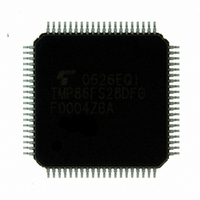
Manufacturer Part Number
TMP86FS28DFG(JZ)
Description
IC MCU 8BIT FLASH 60KB 80-LQFP
Manufacturer
Toshiba
Series
TLCS-870/Cr
Datasheet
1.TMP86FS28DFGJZ.pdf
(272 pages)
Specifications of TMP86FS28DFG(JZ)
Core Processor
870/C
Core Size
8-Bit
Speed
16MHz
Connectivity
SIO, UART/USART
Peripherals
LCD, PWM, WDT
Number Of I /o
62
Program Memory Size
60KB (60K x 8)
Program Memory Type
FLASH
Ram Size
2K x 8
Voltage - Supply (vcc/vdd)
2.7 V ~ 5.5 V
Data Converters
A/D 8x10b
Oscillator Type
Internal
Operating Temperature
-40°C ~ 85°C
Package / Case
80-LQFP
Processor Series
TLCS-870
Core
870/C
Data Bus Width
8 bit
Data Ram Size
2 KB
Interface Type
SIO, UART
Maximum Clock Frequency
16 MHz
Number Of Programmable I/os
62
Number Of Timers
6
Maximum Operating Temperature
+ 85 C
Mounting Style
SMD/SMT
Development Tools By Supplier
BM1040R0A, BMP86A100010A, BMP86A100010B, BMP86A200010B, BMP86A200020A, BMP86A300010A, BMP86A300020A, BMP86A300030A, SW89CN0-ZCC, SW00MN0-ZCC
Minimum Operating Temperature
- 40 C
On-chip Adc
10 bit, 8 Channel
For Use With
BM1401W0A-G - FLASH WRITER ON-BOARD PROGRAMTMP89C900XBG - EMULATION CHIP TMP89F LQFP
Lead Free Status / RoHS Status
Lead free / RoHS Compliant
Eeprom Size
-
Lead Free Status / Rohs Status
Details
Other names
TMP86FS28DFGJZ
Available stocks
Company
Part Number
Manufacturer
Quantity
Price


System Control Register 1
System Control Register 2
SYSCR1
SYSCR2
(0038H)
(0039H)
Note 1: Always set RETM to “0” when transiting from NORMAL mode to STOP mode. Always set RETM to “1” when transiting
Note 2: When STOP mode is released with
Note 3: fc: High-frequency clock [Hz], fs: Low-frequency clock [Hz], *; Don’t care
Note 4: Bits 1 and 0 in SYSCR1 are read as undefined data when a read instruction is executed.
Note 5: As the hardware becomes STOP mode under OUTEN = “0”, input value is fixed to “0”; therefore it may cause external
Note 6: When the key-on wakeup is used, RELM should be set to "1".
Note 7: Port P20 is used as
Note 8: The warmig-up time should be set correctly for using oscillator.
Note 1: A reset is applied if both XEN and XTEN are cleared to “0”, XEN is cleared to “0” when SYSCK = “0”, or XTEN is cleared
Note 2: *: Don’t care, TG: Timing generator, *; Don’t care
Note 3: Bits 3, 1 and 0 in SYSCR2 are always read as undefined value.
Note 4: Do not set IDLE and TGHALT to “1” simultaneously.
Note 5: Because returning from IDLE0/SLEEP0 to NORMAL1/SLOW1 is executed by the asynchronous internal clock, the period
Note 6: When IDLE1/2 or SLEEP1/2 mode is released, IDLE is automatically cleared to “0”.
Note 7: When IDLE0 or SLEEP0 mode is released, TGHALT is automatically cleared to “0”.
Note 8: Before setting TGHALT to “1”, be sure to stop peripherals. If peripherals are not stopped, the interrupt latch of peripherals
from SLOW mode to STOP mode.
interrupt request on account of falling edge.
High-Z mode.
to “0” when SYSCK = “1”.
of IDLE0/SLEEP0 mode might be shorter than the period setting by TBTCR<TBTCK>.
may be set after IDLE0 or SLEEP0 mode is released.
STOP
TGHALT
XEN
SYSCK
OUTEN
XTEN
STOP
RELM
RETM
IDLE
7
7
XEN
WUT
RELM
XTEN
High-frequency oscillator control
Low-frequency oscillator control
Main system clock select
(Write)/main system clock moni-
tor (Read)
CPU and watchdog timer control
(IDLE1/2 and SLEEP1/2 modes)
TG control (IDLE0 and SLEEP0
modes)
6
6
STOP mode start
Release method for STOP
mode
Operating mode after STOP
mode
Port output during STOP mode
Warm-up time at releasing
STOP mode
SYSCK
STOP
RETM
5
5
pin. Therefore, when stop mode is started, OUTEN does not affect to P20, and P20 becomes
OUTEN
IDLE
4
4
RESET
0: CPU core and peripherals remain active
1: CPU core and peripherals are halted (Start STOP mode)
0: Edge-sensitive release
1: Level-sensitive release
0: Return to NORMAL1/2 mode
1: Return to SLOW1 mode
0: High impedance
1: Output kept
0: Turn off oscillation
1: Turn on oscillation
0: Turn off oscillation
1: Turn on oscillation
0: High-frequency clock (NORMAL1/NORMAL2/IDLE1/IDLE2)
1: Low-frequency clock (SLOW1/SLOW2/SLEEP1/SLEEP2)
0: CPU and watchdog timer remain active
1: CPU and watchdog timer are stopped (Start IDLE1/2 and SLEEP1/2 modes)
0: Feeding clock to all peripherals from TG
1: Stop feeding clock to peripherals except TBT from TG.
3
3
pin input, a return is made to NORMAL1 regardless of the RETM contents.
(Start IDLE0 and SLEEP0 modes)
00
01
10
11
WUT
Page 17
TGHALT
2
2
Return to NORMAL mode
3 x 2
3 x 2
1
1
2
2
16
14
16
14
/fc
/fc
/fc
/fc
0
0
(Initial value: 0000 00**)
(Initial value: 1000 *0**)
Return to SLOW mode
3 x 2
3 x 2
2
2
13
6
/fs
13
/fs
6
TMP86FS28DFG
/fs
/fs
R/W
R/W
R/W
R/W
R/W
R/W
R/W
Related parts for TMP86FS28DFG(JZ)
Image
Part Number
Description
Manufacturer
Datasheet
Request
R

Part Number:
Description:
Toshiba Semiconductor [TOSHIBA IGBT Module Silicon N Channel IGBT]
Manufacturer:
TOSHIBA Semiconductor CORPORATION
Datasheet:
Part Number:
Description:
TOSHIBA GTR MODULE SILICON NPN TRIPLE DIFFUSED TYPE
Manufacturer:
TOSHIBA Semiconductor CORPORATION
Datasheet:
Part Number:
Description:
TOSHIBA GTR Module Silicon N Channel IGBT
Manufacturer:
TOSHIBA Semiconductor CORPORATION
Datasheet:
Part Number:
Description:
TOSHIBA Intelligent Power Module Silicon N Channel IGBT
Manufacturer:
TOSHIBA Semiconductor CORPORATION
Datasheet:
Part Number:
Description:
TOSHIBA INTELLIGENT POWER MODULE SILICON N CHANNEL LGBT
Manufacturer:
TOSHIBA Semiconductor CORPORATION
Datasheet:
Part Number:
Description:
TOSHIBA IGBT Module Silicon N Channel IGBT
Manufacturer:
TOSHIBA Semiconductor CORPORATION
Datasheet:
Part Number:
Description:
TOSHIBA GTR MODULE SILICON N−CHANNEL IGBT
Manufacturer:
TOSHIBA Semiconductor CORPORATION
Datasheet:
Part Number:
Description:
TOSHIBA Intelligent Power Module Silicon N Channel IGBT
Manufacturer:
TOSHIBA Semiconductor CORPORATION
Datasheet:
Part Number:
Description:
TOSHIBA GTR Module Silicon N Channel IGBT
Manufacturer:
TOSHIBA Semiconductor CORPORATION
Datasheet:
Part Number:
Description:
TOSHIBA INTELLIGENT POWER MODULE
Manufacturer:
TOSHIBA Semiconductor CORPORATION
Datasheet:
Part Number:
Description:
TOSHIBA Intelligent Power Module Silicon N Channel IGBT
Manufacturer:
TOSHIBA Semiconductor CORPORATION
Datasheet:
Part Number:
Description:
TOSHIBA Intelligent Power Module Silicon N Channel IGBT
Manufacturer:
TOSHIBA Semiconductor CORPORATION
Datasheet:
Part Number:
Description:
TOSHIBA IGBT Module Silicon N Channel IGBT
Manufacturer:
TOSHIBA Semiconductor CORPORATION
Datasheet:
Part Number:
Description:
TOSHIBA Intelligent Power Module Silicon N Channel IGBT
Manufacturer:
TOSHIBA Semiconductor CORPORATION
Datasheet:
Part Number:
Description:
Toshiba Semiconductor [SILICON N CHANNEL 1GBT]
Manufacturer:
TOSHIBA Semiconductor CORPORATION
Datasheet: