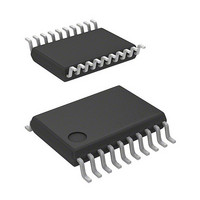
R5F21324CNSP#U0 Renesas Electronics America, R5F21324CNSP#U0 Datasheet - Page 146

R5F21324CNSP#U0
Manufacturer Part Number
R5F21324CNSP#U0
Description
MCU 1KB FLASH 16K ROM 20-LSSOP
Manufacturer
Renesas Electronics America
Series
R8C/3x/32Cr
Datasheet
1.R5F21321CDSPU0.pdf
(605 pages)
Specifications of R5F21324CNSP#U0
Core Processor
R8C
Core Size
16/32-Bit
Speed
20MHz
Connectivity
I²C, LIN, SIO, SSU, UART/USART
Peripherals
POR, PWM, Voltage Detect, WDT
Number Of I /o
15
Program Memory Size
16KB (16K x 8)
Program Memory Type
FLASH
Ram Size
1.5K x 8
Voltage - Supply (vcc/vdd)
1.8 V ~ 5.5 V
Data Converters
A/D 4x10b
Oscillator Type
Internal
Operating Temperature
-20°C ~ 85°C
Package / Case
20-LSSOP
Lead Free Status / RoHS Status
Lead free / RoHS Compliant
Eeprom Size
-
- Current page: 146 of 605
- Download datasheet (6Mb)
R8C/32C Group
REJ09B0573-0100 Rev.1.00 Dec. 18, 2009
Page 117 of 573
Figure 9.10
Table 9.6
Oscillation stop detection
((a) or (b))
Watchdog timer
Voltage monitor 1
Voltage monitor 2
Generated Interrupt Source
Voltage Monitor 1, or Voltage Monitor 2 Interrupt
Procedure for Switching Clock Source from Low-Speed On-Chip Oscillator to XIN
Clock
Determination of Interrupt Sources for Oscillation Stop Detection, Watchdog Timer,
NO
(a) OCD3 bit in OCD register = 1
(b) OCD1 to OCD0 bits in OCD register = 11b and OCD2 bit = 1
VW2C3 bit in VW2C register = 1
VW1C2 bit in VW1C register = 1
VW2C2 bit in VW2C register = 1
Set bits OCD1 to OCD0 to 00b
whether OCD3 bit is set to 0
(XIN clock oscillates)
Check several times
(XIN clock selected)
Switch to XIN clock
Set OCD2 bit to 0
End
YES
Bit Indicating Interrupt Source
OCD3 to OCD0: Bits in OCD register
9. Clock Generation Circuit
Related parts for R5F21324CNSP#U0
Image
Part Number
Description
Manufacturer
Datasheet
Request
R

Part Number:
Description:
KIT STARTER FOR M16C/29
Manufacturer:
Renesas Electronics America
Datasheet:

Part Number:
Description:
KIT STARTER FOR R8C/2D
Manufacturer:
Renesas Electronics America
Datasheet:

Part Number:
Description:
R0K33062P STARTER KIT
Manufacturer:
Renesas Electronics America
Datasheet:

Part Number:
Description:
KIT STARTER FOR R8C/23 E8A
Manufacturer:
Renesas Electronics America
Datasheet:

Part Number:
Description:
KIT STARTER FOR R8C/25
Manufacturer:
Renesas Electronics America
Datasheet:

Part Number:
Description:
KIT STARTER H8S2456 SHARPE DSPLY
Manufacturer:
Renesas Electronics America
Datasheet:

Part Number:
Description:
KIT STARTER FOR R8C38C
Manufacturer:
Renesas Electronics America
Datasheet:

Part Number:
Description:
KIT STARTER FOR R8C35C
Manufacturer:
Renesas Electronics America
Datasheet:

Part Number:
Description:
KIT STARTER FOR R8CL3AC+LCD APPS
Manufacturer:
Renesas Electronics America
Datasheet:

Part Number:
Description:
KIT STARTER FOR RX610
Manufacturer:
Renesas Electronics America
Datasheet:

Part Number:
Description:
KIT STARTER FOR R32C/118
Manufacturer:
Renesas Electronics America
Datasheet:

Part Number:
Description:
KIT DEV RSK-R8C/26-29
Manufacturer:
Renesas Electronics America
Datasheet:

Part Number:
Description:
KIT STARTER FOR SH7124
Manufacturer:
Renesas Electronics America
Datasheet:

Part Number:
Description:
KIT STARTER FOR H8SX/1622
Manufacturer:
Renesas Electronics America
Datasheet:

Part Number:
Description:
KIT DEV FOR SH7203
Manufacturer:
Renesas Electronics America
Datasheet:


