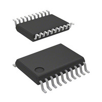
R5F21324CNSP#U0 Renesas Electronics America, R5F21324CNSP#U0 Datasheet - Page 209

R5F21324CNSP#U0
Manufacturer Part Number
R5F21324CNSP#U0
Description
MCU 1KB FLASH 16K ROM 20-LSSOP
Manufacturer
Renesas Electronics America
Series
R8C/3x/32Cr
Datasheet
1.R5F21321CDSPU0.pdf
(605 pages)
Specifications of R5F21324CNSP#U0
Core Processor
R8C
Core Size
16/32-Bit
Speed
20MHz
Connectivity
I²C, LIN, SIO, SSU, UART/USART
Peripherals
POR, PWM, Voltage Detect, WDT
Number Of I /o
15
Program Memory Size
16KB (16K x 8)
Program Memory Type
FLASH
Ram Size
1.5K x 8
Voltage - Supply (vcc/vdd)
1.8 V ~ 5.5 V
Data Converters
A/D 4x10b
Oscillator Type
Internal
Operating Temperature
-20°C ~ 85°C
Package / Case
20-LSSOP
Lead Free Status / RoHS Status
Lead free / RoHS Compliant
Eeprom Size
-
- Current page: 209 of 605
- Download datasheet (6Mb)
R8C/32C Group
REJ09B0573-0100 Rev.1.00 Dec. 18, 2009
Page 180 of 573
Figure 15.9
15.3.5
Table 15.7
j =0 to 23
DTC block size register j
DTC transfer count register j
DTC transfer count reload register j DTRLDj
DTC source address register j
DTC destination address register j
One to 255 bytes of data are transferred by one activation. Either of the transfer source or destination should be
specified as the repeat area. The number of transfer times can be 1 to 255. On completion of the specified
number of transfer times, the DTCCTj (i =0 to 23) register and the address specified for the repeat area are
initialized to continue transfers. When the data transfer causing the DTCCTj register value to change to 0 is
performed while the RPTINT bit in the DTCCRj register is 1 (interrupt generation enabled), an interrupt request
for the CPU is generated during DTC operation.
The lower 8 bits of the initial value for the repeat area address must be 00h. The size of data to be transferred
must be set to 255 bytes or less before the specified number of transfer times is completed.
Table 15.7 shows Register Functions in Repeat Mode.
Figure 15.9 shows Data Transfers in Repeat Mode.
Repeat Mode
DTCCTj register ≠ 1
DTCCTj register = 1
Register
Register Functions in Repeat Mode
Data Transfers in Repeat Mode
SRC0: Initial source address value
DST0: Initial destination address value
X: 0 or 1
X: 0 or 1
DTCCR register
DTCCR register
Bits b3 to b0 in
Bits b3 to b0 in
0X11b
1X11b
X001b
X101b
0X11b
1X11b
X001b
X101b
Transfer source
SRC
Source address
Source address
Repeat area
Repeat area
Incremented
Repeat area
Repeat area
Incremented
control
control
Fixed
Fixed
DTBLSj
DTCCTj
DTSARj
DTDARj
Symbol
Destination address
Destination address
Transfer
Incremented
Repeat area
Repeat area
Incremented
Repeat area
Repeat area
control
control
Fixed
Fixed
SRC0/DST0
Repeat area
SRC/DST
Size of the data block to be transferred by one activation
Number of times of data transfers
This register value is reloaded to the DTCCT register. (Data
transfer count is initialized.)
Data transfer source address
Data transfer destination address
Transfer destination
DST
Source address
Source address
after transfer
after transfer
SRC+N
SRC+N
SRC+N
SRC+N
SRC0
SRC0
SRC
SRC
Address of the repeat area is initialized
after a transfer.
DTBLSj = N
DTCCTj = 1
DTSARj = SRC
DTDARj = DST
j = 0 to 23
Size of the data block to be transferred by
one activation (N bytes)
DTBLSj = N
DTCCTj ≠ 1
DTSARj = SRC
DTDARj = DST
j = 0 to 23
Destination address
Destination address
Function
after transfer
after transfer
DST+N
DST+N
DST+N
DST+N
DST0
DST0
DST
DST
15. DTC
Related parts for R5F21324CNSP#U0
Image
Part Number
Description
Manufacturer
Datasheet
Request
R

Part Number:
Description:
KIT STARTER FOR M16C/29
Manufacturer:
Renesas Electronics America
Datasheet:

Part Number:
Description:
KIT STARTER FOR R8C/2D
Manufacturer:
Renesas Electronics America
Datasheet:

Part Number:
Description:
R0K33062P STARTER KIT
Manufacturer:
Renesas Electronics America
Datasheet:

Part Number:
Description:
KIT STARTER FOR R8C/23 E8A
Manufacturer:
Renesas Electronics America
Datasheet:

Part Number:
Description:
KIT STARTER FOR R8C/25
Manufacturer:
Renesas Electronics America
Datasheet:

Part Number:
Description:
KIT STARTER H8S2456 SHARPE DSPLY
Manufacturer:
Renesas Electronics America
Datasheet:

Part Number:
Description:
KIT STARTER FOR R8C38C
Manufacturer:
Renesas Electronics America
Datasheet:

Part Number:
Description:
KIT STARTER FOR R8C35C
Manufacturer:
Renesas Electronics America
Datasheet:

Part Number:
Description:
KIT STARTER FOR R8CL3AC+LCD APPS
Manufacturer:
Renesas Electronics America
Datasheet:

Part Number:
Description:
KIT STARTER FOR RX610
Manufacturer:
Renesas Electronics America
Datasheet:

Part Number:
Description:
KIT STARTER FOR R32C/118
Manufacturer:
Renesas Electronics America
Datasheet:

Part Number:
Description:
KIT DEV RSK-R8C/26-29
Manufacturer:
Renesas Electronics America
Datasheet:

Part Number:
Description:
KIT STARTER FOR SH7124
Manufacturer:
Renesas Electronics America
Datasheet:

Part Number:
Description:
KIT STARTER FOR H8SX/1622
Manufacturer:
Renesas Electronics America
Datasheet:

Part Number:
Description:
KIT DEV FOR SH7203
Manufacturer:
Renesas Electronics America
Datasheet:


