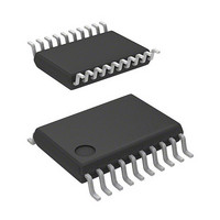
R5F21324CNSP#U0 Renesas Electronics America, R5F21324CNSP#U0 Datasheet - Page 366

R5F21324CNSP#U0
Manufacturer Part Number
R5F21324CNSP#U0
Description
MCU 1KB FLASH 16K ROM 20-LSSOP
Manufacturer
Renesas Electronics America
Series
R8C/3x/32Cr
Datasheet
1.R5F21321CDSPU0.pdf
(605 pages)
Specifications of R5F21324CNSP#U0
Core Processor
R8C
Core Size
16/32-Bit
Speed
20MHz
Connectivity
I²C, LIN, SIO, SSU, UART/USART
Peripherals
POR, PWM, Voltage Detect, WDT
Number Of I /o
15
Program Memory Size
16KB (16K x 8)
Program Memory Type
FLASH
Ram Size
1.5K x 8
Voltage - Supply (vcc/vdd)
1.8 V ~ 5.5 V
Data Converters
A/D 4x10b
Oscillator Type
Internal
Operating Temperature
-20°C ~ 85°C
Package / Case
20-LSSOP
Lead Free Status / RoHS Status
Lead free / RoHS Compliant
Eeprom Size
-
- Current page: 366 of 605
- Download datasheet (6Mb)
R8C/32C Group
REJ09B0573-0100 Rev.1.00 Dec. 18, 2009
Page 337 of 573
Figure 22.8
22.4.1
Table 22.8
Note:
Bit Rate
115200
14400
19200
28800
38400
57600
(bps)
1200
2400
4800
9600
Receive Timing Example When Transfer Data 8 Bits is Long (Parity Disabled, One Stop Bit)
1. For the high-speed on-chip oscillator, the correction value in the FRA4 register should be written into the FRA1
S2RIC register
In UART mode, the bit rate is the frequency divided by the U2BRG register divided by 16. Table 22.8 lists the
Bit Rate Setting Example in UART Mode (Internal Clock Selected).
U2C1 register
U2C1 register
Transfer clock
register and the correction value in the FRA5 register should be written into the FRA3 register.
This applies when the high-speed on-chip oscillator is selected as the system clock and bits FRA22 to FRA20
in the FRA2 register are set to 000b (divide-by-2 mode). For the precision of the high-speed on-chip oscillator,
refer to 31. Electrical Characteristics .
count source
U2BRG
Source
RE bit in
Count
U2BRG
RI bit in
IR bit in
Bit Rate
RXD2
f8
f8
f8
f1
f1
f1
f1
f1
f1
f1
RTS2
Bit Rate Setting Example in UART Mode (Internal Clock Selected)
Receive Timing in UART Mode
The above applies when:
• PRYE bit in U2MR register = 0 (parity disabled)
• STPS bit in U2MR register = 0 (one stop bit)
• CRD bit in U2C0 register = 0 (CTS2/RTS2 function enabled), CRS bit = 1 (RTS2 function selected)
129 (81h)
129 (81h)
64 (40h)
32 (20h)
86 (56h)
64 (40h)
42 (2Ah)
32 (20h)
21 (15h)
10 (0Ah)
U2BRG
Setting
Value
System Clock = 20 MHz
Reception starts when a transfer clock
is generated at the falling edge
of the start bit.
113636.36
Start bit
14367.82
19230.77
29069.77
37878.79
56818.18
Actual
(bps)
Time
1201.92
2403.85
4734.85
9615.38
“L” is determined.
Setting
Error
(%)
-1.36 29 (1Dh)
-0.22 79 (4Fh)
-1.36 29 (1Dh)
-1.36 19 (13h)
-1.36
0.16 119 (77h)
0.16 59 (3Bh)
0.16 119 (77h)
0.16 59 (3Bh)
0.94 39 (27h)
System Clock = 18.432 MHz
U2BRG
9 (09h)
Setting
Value
D0
Set to 0 when an interrupt request is acknowledged or by a program.
Receive data taken in
Data transfer from UART2 receive register
to U2RB register
115200.00
14400.00
19200.00
28800.00
38400.00
57600.00
Actual
Time
(bps)
1200.00
2400.00
4800.00
9600.00
D1
Setting
Error
D7
(%)
0.00 51 (33h)
0.00 25 (19h)
0.00 12 (0Ch)
0.00 51 (33h)
0.00 34 (22h)
0.00 25 (19h)
0.00 16 (10h)
0.00 12 (0Ch)
0.00
0.00
(1)
U2BRG
8 (08h)
Setting
Value
22. Serial Interface (UART2)
System Clock = 8 MHz
−
Stop bit
14285.71
19230.77
29411.76
38461.54
55555.56
Actual
Time
(bps)
1201.92
2403.85
4807.69
9615.38
−
Setting
Error
(%)
-0.79
-3.55
0.16
0.16
0.16
0.16
0.16
2.12
0.16
−
Related parts for R5F21324CNSP#U0
Image
Part Number
Description
Manufacturer
Datasheet
Request
R

Part Number:
Description:
KIT STARTER FOR M16C/29
Manufacturer:
Renesas Electronics America
Datasheet:

Part Number:
Description:
KIT STARTER FOR R8C/2D
Manufacturer:
Renesas Electronics America
Datasheet:

Part Number:
Description:
R0K33062P STARTER KIT
Manufacturer:
Renesas Electronics America
Datasheet:

Part Number:
Description:
KIT STARTER FOR R8C/23 E8A
Manufacturer:
Renesas Electronics America
Datasheet:

Part Number:
Description:
KIT STARTER FOR R8C/25
Manufacturer:
Renesas Electronics America
Datasheet:

Part Number:
Description:
KIT STARTER H8S2456 SHARPE DSPLY
Manufacturer:
Renesas Electronics America
Datasheet:

Part Number:
Description:
KIT STARTER FOR R8C38C
Manufacturer:
Renesas Electronics America
Datasheet:

Part Number:
Description:
KIT STARTER FOR R8C35C
Manufacturer:
Renesas Electronics America
Datasheet:

Part Number:
Description:
KIT STARTER FOR R8CL3AC+LCD APPS
Manufacturer:
Renesas Electronics America
Datasheet:

Part Number:
Description:
KIT STARTER FOR RX610
Manufacturer:
Renesas Electronics America
Datasheet:

Part Number:
Description:
KIT STARTER FOR R32C/118
Manufacturer:
Renesas Electronics America
Datasheet:

Part Number:
Description:
KIT DEV RSK-R8C/26-29
Manufacturer:
Renesas Electronics America
Datasheet:

Part Number:
Description:
KIT STARTER FOR SH7124
Manufacturer:
Renesas Electronics America
Datasheet:

Part Number:
Description:
KIT STARTER FOR H8SX/1622
Manufacturer:
Renesas Electronics America
Datasheet:

Part Number:
Description:
KIT DEV FOR SH7203
Manufacturer:
Renesas Electronics America
Datasheet:


