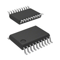
R5F21324CNSP#U0 Renesas Electronics America, R5F21324CNSP#U0 Datasheet - Page 75

R5F21324CNSP#U0
Manufacturer Part Number
R5F21324CNSP#U0
Description
MCU 1KB FLASH 16K ROM 20-LSSOP
Manufacturer
Renesas Electronics America
Series
R8C/3x/32Cr
Datasheet
1.R5F21321CDSPU0.pdf
(605 pages)
Specifications of R5F21324CNSP#U0
Core Processor
R8C
Core Size
16/32-Bit
Speed
20MHz
Connectivity
I²C, LIN, SIO, SSU, UART/USART
Peripherals
POR, PWM, Voltage Detect, WDT
Number Of I /o
15
Program Memory Size
16KB (16K x 8)
Program Memory Type
FLASH
Ram Size
1.5K x 8
Voltage - Supply (vcc/vdd)
1.8 V ~ 5.5 V
Data Converters
A/D 4x10b
Oscillator Type
Internal
Operating Temperature
-20°C ~ 85°C
Package / Case
20-LSSOP
Lead Free Status / RoHS Status
Lead free / RoHS Compliant
Eeprom Size
-
- Current page: 75 of 605
- Download datasheet (6Mb)
R8C/32C Group
REJ09B0573-0100 Rev.1.00 Dec. 18, 2009
Page 46 of 573
6.2.7
Notes:
After Reset
1. The VW1C0 is enabled when the VCA26 bit in the VCA2 register is set to 1 (voltage detection 1 circuit enabled).
2. When using the digital filter (while the VW1C1 bit is 0), set the CM14 bit in the CM1 register to 0 (low-speed on-
3. Bits VW1C2 and VW1C3 are enabled when the VCA26 bit in the VCA2 register is set to 1 (voltage detection 1
4. Set the VW1C2 bit to 0 by a program. When 0 is written by a program, this bit is set to 0 (and remains unchanged
5. The VW1C7 bit is enabled when the VCAC1 bit in the VCAC register is set to 0 (one edge). After setting the
6. When the VW1C0 bit is set to 1 (enabled), do not set the VW1C1 bit and bits VW1F1 and VW1F0 simultaneously
Bit
b0
b1
b2
b3
b4
b5
b6
b7
Address 0039h
Symbol VW1C7
Set the VW1C0 bit to 0 (disabled) when the VCA26 bit is set to 0 (voltage detection 1 circuit disabled).
To set the VW0C0 bit to 1 (enabled), follow the procedure shown in Table 6.2 Procedure for Setting Bits
Associated with Voltage Monitor 1 Interrupt.
chip oscillator on).
To use the voltage monitor 1 interrupt to exit stop mode, set the VW1C1 bit in the VW1C register to 1 (digital filter
disabled).
circuit enabled).
even if 1 is written to it).
VCAC1 bit to 0, set the VW1C7 bit.
(with one instruction).
Set the PRC3 bit in the PRCR register to 1 (write enabled) before writing the VW1C register.
Rewriting the VW1C register may set the VW1C2 bit to 1. Set the VW1C2 bit to 0 after rewriting the VW1C
register.
Bit
VW1C0 Voltage monitor 1 reset interrupt enable
VW1C1 Voltage monitor 1 digital filter
VW1C2 Voltage change detection flag
VW1C3 Voltage detection 1 signal monitor flag
VW1C7 Voltage monitor 1 interrupt
Symbol
VW1F0 Sampling clock select bit
VW1F1
Voltage Monitor 1 Circuit Control Register (VW1C)
—
b7
1
bit
disable mode select bit
Reserved bit
generation condition select bit
(1)
b6
—
0
VW1F1
Bit Name
b5
0
(2, 6)
(6)
VW1F0
b4
0
(3, 4)
(5)
VW1C3
(3)
b3
1
0: Disabled
1: Enabled
0: Digital filter enabled mode
1: Digital filter disable mode
0: Not detected
1: Vdet1 passing detected
0: VCC
1: VCC
b5 b4
Set to 0.
0: When VCC reaches Vdet1 or above.
1: When VCC reaches Vdet1 or below.
0 0: fOCO-S divided by 1
0 1: fOCO-S divided by 2
1 0: fOCO-S divided by 4
1 1: fOCO-S divided by 8
(digital filter circuit enabled)
(digital filter circuit disabled)
or voltage detection 1 circuit disabled
VW1C2
b2
<
≥
0
Vdet1
Vdet1
VW1C1
b1
1
Function
VW1C0
6. Voltage Detection Circuit
b0
0
R/W
R/W
R/W
R/W
R/W
R/W
R/W
R/W
R
Related parts for R5F21324CNSP#U0
Image
Part Number
Description
Manufacturer
Datasheet
Request
R

Part Number:
Description:
KIT STARTER FOR M16C/29
Manufacturer:
Renesas Electronics America
Datasheet:

Part Number:
Description:
KIT STARTER FOR R8C/2D
Manufacturer:
Renesas Electronics America
Datasheet:

Part Number:
Description:
R0K33062P STARTER KIT
Manufacturer:
Renesas Electronics America
Datasheet:

Part Number:
Description:
KIT STARTER FOR R8C/23 E8A
Manufacturer:
Renesas Electronics America
Datasheet:

Part Number:
Description:
KIT STARTER FOR R8C/25
Manufacturer:
Renesas Electronics America
Datasheet:

Part Number:
Description:
KIT STARTER H8S2456 SHARPE DSPLY
Manufacturer:
Renesas Electronics America
Datasheet:

Part Number:
Description:
KIT STARTER FOR R8C38C
Manufacturer:
Renesas Electronics America
Datasheet:

Part Number:
Description:
KIT STARTER FOR R8C35C
Manufacturer:
Renesas Electronics America
Datasheet:

Part Number:
Description:
KIT STARTER FOR R8CL3AC+LCD APPS
Manufacturer:
Renesas Electronics America
Datasheet:

Part Number:
Description:
KIT STARTER FOR RX610
Manufacturer:
Renesas Electronics America
Datasheet:

Part Number:
Description:
KIT STARTER FOR R32C/118
Manufacturer:
Renesas Electronics America
Datasheet:

Part Number:
Description:
KIT DEV RSK-R8C/26-29
Manufacturer:
Renesas Electronics America
Datasheet:

Part Number:
Description:
KIT STARTER FOR SH7124
Manufacturer:
Renesas Electronics America
Datasheet:

Part Number:
Description:
KIT STARTER FOR H8SX/1622
Manufacturer:
Renesas Electronics America
Datasheet:

Part Number:
Description:
KIT DEV FOR SH7203
Manufacturer:
Renesas Electronics America
Datasheet:


