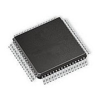
MC908LJ24CFUER Freescale Semiconductor, MC908LJ24CFUER Datasheet - Page 297

MC908LJ24CFUER
Manufacturer Part Number
MC908LJ24CFUER
Description
IC MCU 24K FLASH 8MHZ SPI 64-QFP
Manufacturer
Freescale Semiconductor
Series
HC08r
Datasheet
1.MC908LK24CFUE.pdf
(464 pages)
Specifications of MC908LJ24CFUER
Core Processor
HC08
Core Size
8-Bit
Speed
8MHz
Connectivity
I²C, IRSCI, SPI
Peripherals
LCD, LVD, POR, PWM
Number Of I /o
40
Program Memory Size
24KB (24K x 8)
Program Memory Type
FLASH
Ram Size
768 x 8
Voltage - Supply (vcc/vdd)
3 V ~ 5.5 V
Data Converters
A/D 6x10b
Oscillator Type
Internal
Operating Temperature
-40°C ~ 85°C
Package / Case
64-QFP
Processor Series
HC08LJ
Core
HC08
Data Bus Width
8 bit
Data Ram Size
768 B
Interface Type
SCI, SPI
Maximum Clock Frequency
8 MHz
Number Of Programmable I/os
48
Number Of Timers
4
Maximum Operating Temperature
+ 85 C
Mounting Style
SMD/SMT
Development Tools By Supplier
FSICEBASE, M68EML08LJLKE, ZK-HC08LX-A, M68CBL05CE
Minimum Operating Temperature
- 40 C
On-chip Adc
10 bit, 6 Channel
Lead Free Status / RoHS Status
Lead free / RoHS Compliant
Eeprom Size
-
Lead Free Status / Rohs Status
Details
Available stocks
Company
Part Number
Manufacturer
Quantity
Price
Company:
Part Number:
MC908LJ24CFUER
Manufacturer:
Freescale Semiconductor
Quantity:
10 000
- Current page: 297 of 464
- Download datasheet (5Mb)
14.6.4 Transmission Initiation Latency
MC68HC908LJ24/LK24 — Rev. 2.1
Freescale Semiconductor
When CPHA = 1 for a slave, the first edge of the SPSCK indicates the
beginning of the transmission. This causes the SPI to leave its idle state
and begin driving the MISO pin with the MSB of its data. Once the
transmission begins, no new data is allowed into the shift register from
the transmit data register. Therefore, the SPI data register of the slave
must be loaded with transmit data before the first edge of SPSCK. Any
data written after the first edge is stored in the transmit data register and
transferred to the shift register after the current transmission.
When the SPI is configured as a master (SPMSTR = 1), writing to the
SPDR starts a transmission. CPHA has no effect on the delay to the start
of the transmission, but it does affect the initial state of the SPSCK
signal. When CPHA = 0, the SPSCK signal remains inactive for the first
half of the first SPSCK cycle. When CPHA = 1, the first SPSCK cycle
begins with an edge on the SPSCK line from its inactive to its active
level. The SPI clock rate (selected by SPR1:SPR0) affects the delay
from the write to SPDR and the start of the SPI transmission. (See
Figure
derivative of the internal MCU clock. To conserve power, it is enabled
only when both the SPE and SPMSTR bits are set. SPSCK edges occur
halfway through the low time of the internal MCU clock. Since the SPI
clock is free-running, it is uncertain where the write to the SPDR occurs
relative to the slower SPSCK. This uncertainty causes the variation in
the initiation delay shown in
single SPI bit time. That is, the maximum delay is two MCU bus cycles
for DIV2, eight MCU bus cycles for DIV8, 32 MCU bus cycles for DIV32,
and 128 MCU bus cycles for DIV128.
Serial Peripheral Interface Module (SPI)
14-7.) The internal SPI clock in the master is a free-running
Figure
14-7. This delay is no longer than a
Serial Peripheral Interface Module (SPI)
Transmission Formats
Data Sheet
297
Related parts for MC908LJ24CFUER
Image
Part Number
Description
Manufacturer
Datasheet
Request
R
Part Number:
Description:
Manufacturer:
Freescale Semiconductor, Inc
Datasheet:
Part Number:
Description:
Manufacturer:
Freescale Semiconductor, Inc
Datasheet:
Part Number:
Description:
Manufacturer:
Freescale Semiconductor, Inc
Datasheet:
Part Number:
Description:
Manufacturer:
Freescale Semiconductor, Inc
Datasheet:
Part Number:
Description:
Manufacturer:
Freescale Semiconductor, Inc
Datasheet:
Part Number:
Description:
Manufacturer:
Freescale Semiconductor, Inc
Datasheet:
Part Number:
Description:
Manufacturer:
Freescale Semiconductor, Inc
Datasheet:
Part Number:
Description:
Manufacturer:
Freescale Semiconductor, Inc
Datasheet:
Part Number:
Description:
Manufacturer:
Freescale Semiconductor, Inc
Datasheet:
Part Number:
Description:
Manufacturer:
Freescale Semiconductor, Inc
Datasheet:
Part Number:
Description:
Manufacturer:
Freescale Semiconductor, Inc
Datasheet:
Part Number:
Description:
Manufacturer:
Freescale Semiconductor, Inc
Datasheet:
Part Number:
Description:
Manufacturer:
Freescale Semiconductor, Inc
Datasheet:
Part Number:
Description:
Manufacturer:
Freescale Semiconductor, Inc
Datasheet:
Part Number:
Description:
Manufacturer:
Freescale Semiconductor, Inc
Datasheet:


