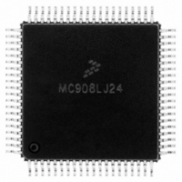
MC908LJ24CFQE Freescale Semiconductor, MC908LJ24CFQE Datasheet - Page 289

MC908LJ24CFQE
Manufacturer Part Number
MC908LJ24CFQE
Description
IC MCU 24K FLASH 8MHZ SPI 80-QFP
Manufacturer
Freescale Semiconductor
Series
HC08r
Datasheet
1.MC908LK24CFUE.pdf
(464 pages)
Specifications of MC908LJ24CFQE
Core Processor
HC08
Core Size
8-Bit
Speed
8MHz
Connectivity
I²C, IRSCI, SPI
Peripherals
LCD, LVD, POR, PWM
Number Of I /o
48
Program Memory Size
24KB (24K x 8)
Program Memory Type
FLASH
Ram Size
768 x 8
Voltage - Supply (vcc/vdd)
3 V ~ 5.5 V
Data Converters
A/D 6x10b
Oscillator Type
Internal
Operating Temperature
-40°C ~ 85°C
Package / Case
80-QFP
Controller Family/series
HC08
No. Of I/o's
48
Ram Memory Size
768Byte
Cpu Speed
8MHz
No. Of Timers
2
Embedded Interface Type
I2C, SCI, SPI
Rohs Compliant
Yes
Processor Series
HC08LJ
Core
HC08
Data Bus Width
8 bit
Data Ram Size
768 B
Interface Type
SCI, SPI
Maximum Clock Frequency
8 MHz
Number Of Programmable I/os
48
Number Of Timers
4
Operating Supply Voltage
0 V to 5 V
Maximum Operating Temperature
+ 85 C
Mounting Style
SMD/SMT
Development Tools By Supplier
FSICEBASE, M68EML08LJLKE, ZK-HC08LX-A, M68CBL05CE
Minimum Operating Temperature
- 40 C
On-chip Adc
10 bit, 6 Channel
Lead Free Status / RoHS Status
Lead free / RoHS Compliant
Eeprom Size
-
Lead Free Status / Rohs Status
Details
Available stocks
Company
Part Number
Manufacturer
Quantity
Price
Company:
Part Number:
MC908LJ24CFQE
Manufacturer:
Freescale Semiconductor
Quantity:
10 000
- Current page: 289 of 464
- Download datasheet (5Mb)
14.4 Pin Name Conventions and I/O Register Addresses
MC68HC908LJ24/LK24 — Rev. 2.1
Freescale Semiconductor
Addr.
$0010
$0011
$0012
SPI Status and Control
Register Name
SPI Control Register
SPI Data Register
NOTE:
(SPSCR)
Register
(SPCR)
(SPDR)
The text that follows describes the SPI. The SPI I/O pin names are SS
(slave select), SPSCK (SPI serial clock), CGND (clock ground), MOSI
(master out slave in), and MISO (master in/slave out). The SPI shares
four I/O pins with four parallel I/O ports.
The full names of the SPI I/O pins are shown in
pin names appear in the text that follows.
The SS and SPSCK pins are also shared with CALIN and CALOUT
respectively. To avoid erratic behavior, these two pins should never be
configured for use as SPI and RTC calibration simultaneously.
Figure 14-1
=
Pin Names: SPI PTD1/MISO PTD2/MOSI
Reset:
Reset:
Reset:
Read:
Read:
Read:
Write:
Write:
Write:
Full SPI
SPI Generic
Figure 14-1. SPI I/O Register Summary
Pin Names:
Serial Peripheral Interface Module (SPI)
SPRIE
SPRF
Bit 7
R7
T7
0
0
summarizes the SPI I/O registers.
= Unimplemented
ERRIE
Table 14-1. Pin Name Conventions
R6
T6
R
6
0
0
MISO
SPMSTR
OVRF
R5
T5
5
1
0
Pin Name Conventions and I/O Register Addresses
Unaffected by reset
MOSI
MODF
CPOL
R4
T4
4
0
0
Serial Peripheral Interface Module (SPI)
CPHA
SPTE
PTD0/SS
R3
T3
R
3
1
1
CALIN
SS
Table
= Reserved
SPWOM
MODFEN
R2
T2
2
0
0
PTD3/SPSCK/
14-1. The generic
CALOUT
SPSCK
SPR1
SPE
R1
T1
1
0
0
Data Sheet
CGND
SPTIE
SPR0
Bit 0
V
R0
T0
0
0
SS
289
Related parts for MC908LJ24CFQE
Image
Part Number
Description
Manufacturer
Datasheet
Request
R
Part Number:
Description:
Manufacturer:
Freescale Semiconductor, Inc
Datasheet:
Part Number:
Description:
Manufacturer:
Freescale Semiconductor, Inc
Datasheet:
Part Number:
Description:
Manufacturer:
Freescale Semiconductor, Inc
Datasheet:
Part Number:
Description:
Manufacturer:
Freescale Semiconductor, Inc
Datasheet:
Part Number:
Description:
Manufacturer:
Freescale Semiconductor, Inc
Datasheet:
Part Number:
Description:
Manufacturer:
Freescale Semiconductor, Inc
Datasheet:
Part Number:
Description:
Manufacturer:
Freescale Semiconductor, Inc
Datasheet:
Part Number:
Description:
Manufacturer:
Freescale Semiconductor, Inc
Datasheet:
Part Number:
Description:
Manufacturer:
Freescale Semiconductor, Inc
Datasheet:
Part Number:
Description:
Manufacturer:
Freescale Semiconductor, Inc
Datasheet:
Part Number:
Description:
Manufacturer:
Freescale Semiconductor, Inc
Datasheet:
Part Number:
Description:
Manufacturer:
Freescale Semiconductor, Inc
Datasheet:
Part Number:
Description:
Manufacturer:
Freescale Semiconductor, Inc
Datasheet:
Part Number:
Description:
Manufacturer:
Freescale Semiconductor, Inc
Datasheet:
Part Number:
Description:
Manufacturer:
Freescale Semiconductor, Inc
Datasheet:


