R5F21272SNFP#U0 Renesas Electronics America, R5F21272SNFP#U0 Datasheet - Page 105
R5F21272SNFP#U0
Manufacturer Part Number
R5F21272SNFP#U0
Description
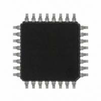
IC R8C/27 MCU FLASH 32LQFP
Manufacturer
Renesas Electronics America
Series
R8C/2x/27r
Datasheet
1.R5F21272SDFPU0.pdf
(487 pages)
Specifications of R5F21272SNFP#U0
Core Processor
R8C
Core Size
16/32-Bit
Speed
20MHz
Connectivity
I²C, LIN, SIO, SSU, UART/USART
Peripherals
LED, POR, Voltage Detect, WDT
Number Of I /o
25
Program Memory Size
8KB (8K x 8)
Program Memory Type
FLASH
Ram Size
512 x 8
Voltage - Supply (vcc/vdd)
2.2 V ~ 5.5 V
Data Converters
A/D 12x10b
Oscillator Type
Internal
Operating Temperature
-20°C ~ 85°C
Package / Case
32-LQFP
For Use With
R0K521276S000BE - KIT DEV RSK-R8C/26-29R0E521000EPB00 - PROBE EMULATOR FOR PC7501
Lead Free Status / RoHS Status
Lead free / RoHS Compliant
Eeprom Size
-
Available stocks
Company
Part Number
Manufacturer
Quantity
Price

Part Number:
R5F21272SNFP#U0R5F21272SNFP#V2
Manufacturer:
Renesas Electronics America
Quantity:
10 000


R8C/26 Group, R8C/27 Group
Rev.2.10
REJ09B0278-0210
Figure 10.7
Figure 10.8
Clock Prescaler Reset Flag (For N, D Version Only)
Voltage Detection Register 2
b7 b6 b5 b4 b3 b2 b1 b0
NOTE:
b7 b6 b5 b4
NOTES:
1.
1.
2.
3.
4.
5.
6. Use the VCA20 bit only w hen entering to w ait mode. To set the VCA20 bit, follow the procedure show n in Figure
0 0 0 0 0 0 0
Only w rite 1 to this bit w hen selecting the XCIN clock as the CPU clock, .
Set the PRC3 bit in the PRCR register to 1 (w rite enable) before w riting to the VCA2 register.
To use the voltage monitor 0 reset, set the VCA25 bit to 1.
After the VCA25 bit is set to 1 from 0, the voltage detection circuit w aits for td(E-A) to elapse before starting
operation.
To use the voltage monitor 1 interrupt/reset or the VW1C3 bit in the VW1C register, set the VCA26 bit to 1.
After the VCA26 bit is set to 1 from 0, the voltage detection circuit w aits for td(E-A) to elapse before starting
operation.
To use the voltage monitor 2 interrupt/reset or the VCA13 bit in the VCA1 register, set the VCA27 bit to 1.
After the VCA27 bit is set to 1 from 0, the voltage detection circuit w aits for td(E-A) to elapse before starting
operation.
Softw are reset, w atchdog timer reset, voltage monitor 1 reset, and voltage monitor 2 reset do not affect this
register.
10.10 Procedure for Enabling Reduced Internal Pow er Consum ption Using VCA20 bit.
Sep 26, 2008
0
b3 b2 b1 b0
0 0 0
CPSRF Register
VCA2 Register (N, D Version)
Bit Symbol
Bit Symbol
(b6-b0)
VCA20
(b4-b1)
VCA25
VCA26
VCA27
Symbol
Symbol
CPSRF
VCA2
CPSR
Page 86 of 453
—
—
(1)
Reserved bits
Clock prescaler reset flag
Internal pow er low
consumption enable bit
Reserved bits
Voltage detection 0 enable
bit
Voltage detection 1 enable
bit
Voltage detection 2 enable
bit
(N, D Version)
(2)
(3)
(4)
Address
Bit Name
0032h
Address
Bit Name
0028h
(6)
(1)
The LVD0ON bit in the OFS register is
set to 1 and hardw are reset
Pow er-on reset, voltage monitor 0 reset
or LVD0ON bit in the OFS register is
set to 0, and hardw are reset
0 : Disables low consumption
1 : Enables low consumption
Set to 0.
0 : Voltage detection 0 circuit disabled
1 : Voltage detection 0 circuit enabled
0 : Voltage detection 1 circuit disabled
1 : Voltage detection 1 circuit enabled
0 : Voltage detection 2 circuit disabled
1 : Voltage detection 2 circuit enabled
Set to 0.
Setting this bit to 1 initializes the clock
prescaler. (When read, the content is 0)
After Reset
Function
After Reset
Function
00h
10. Clock Generation Circuit
(5)
: 00h
: 00100000b
RW
RW
RW
RW
RW
RW
RW
RW
RW
Related parts for R5F21272SNFP#U0
Image
Part Number
Description
Manufacturer
Datasheet
Request
R

Part Number:
Description:
KIT STARTER FOR M16C/29
Manufacturer:
Renesas Electronics America
Datasheet:

Part Number:
Description:
KIT STARTER FOR R8C/2D
Manufacturer:
Renesas Electronics America
Datasheet:

Part Number:
Description:
R0K33062P STARTER KIT
Manufacturer:
Renesas Electronics America
Datasheet:

Part Number:
Description:
KIT STARTER FOR R8C/23 E8A
Manufacturer:
Renesas Electronics America
Datasheet:

Part Number:
Description:
KIT STARTER FOR R8C/25
Manufacturer:
Renesas Electronics America
Datasheet:

Part Number:
Description:
KIT STARTER H8S2456 SHARPE DSPLY
Manufacturer:
Renesas Electronics America
Datasheet:

Part Number:
Description:
KIT STARTER FOR R8C38C
Manufacturer:
Renesas Electronics America
Datasheet:

Part Number:
Description:
KIT STARTER FOR R8C35C
Manufacturer:
Renesas Electronics America
Datasheet:

Part Number:
Description:
KIT STARTER FOR R8CL3AC+LCD APPS
Manufacturer:
Renesas Electronics America
Datasheet:
Part Number:
Description:
KIT STARTER FOR RX610
Manufacturer:
Renesas Electronics America
Datasheet:

Part Number:
Description:
KIT STARTER FOR R32C/118
Manufacturer:
Renesas Electronics America
Datasheet:

Part Number:
Description:
KIT DEV RSK-R8C/26-29
Manufacturer:
Renesas Electronics America
Datasheet:

Part Number:
Description:
KIT STARTER FOR SH7124
Manufacturer:
Renesas Electronics America
Datasheet:

Part Number:
Description:
KIT STARTER FOR H8SX/1622
Manufacturer:
Renesas Electronics America
Datasheet:

Part Number:
Description:
KIT DEV FOR SH7203
Manufacturer:
Renesas Electronics America
Datasheet: