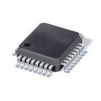
C8051F350-GQR Silicon Laboratories Inc, C8051F350-GQR Datasheet

C8051F350-GQR
Manufacturer Part Number
C8051F350-GQR
Description
IC 8051 MCU 8K FLASH 32LQFP
Manufacturer
Silicon Laboratories Inc
Series
C8051F35xr
Specifications of C8051F350-GQR
Core Processor
8051
Core Size
8-Bit
Speed
50MHz
Connectivity
SMBus (2-Wire/I²C), SPI, UART/USART
Peripherals
POR, PWM, Temp Sensor, WDT
Number Of I /o
17
Program Memory Size
8KB (8K x 8)
Program Memory Type
FLASH
Ram Size
768 x 8
Voltage - Supply (vcc/vdd)
2.7 V ~ 3.6 V
Data Converters
A/D 8x24b; D/A 2x8b
Oscillator Type
Internal
Operating Temperature
-40°C ~ 85°C
Package / Case
32-LQFP
Core
8051
Processor Series
C8051F3x
Data Bus Width
8 bit
Maximum Clock Frequency
50 MHz
Data Ram Size
768 B
Data Rom Size
128 B
On-chip Adc
Yes
Number Of Programmable I/os
17
Number Of Timers
4 bit
Operating Supply Voltage
2.7 V to 3.6 V
Mounting Style
SMD/SMT
A/d Bit Size
24 bit
A/d Channels Available
8
Height
1.4 mm
Interface Type
I2C, SMBus, SPI, UART
Length
7 mm
Maximum Operating Temperature
+ 85 C
Minimum Operating Temperature
- 40 C
Supply Voltage (max)
3.6 V
Supply Voltage (min)
2.7 V
Width
7 mm
For Use With
336-1165 - KIT REFERENCE DESIGN DGTL COMPSS336-1083 - DEV KIT FOR F350/351/352/353
Lead Free Status / RoHS Status
Lead free / RoHS Compliant
Eeprom Size
-
Lead Free Status / Rohs Status
Details
Available stocks
Company
Part Number
Manufacturer
Quantity
Price
Company:
Part Number:
C8051F350-GQR
Manufacturer:
Silicon Laboratories Inc
Quantity:
10 000
Part Number:
C8051F350-GQR
Manufacturer:
SILICON LABS/芯科
Quantity:
20 000
Analog Peripherals
24-Bit ADC
-
-
-
-
-
-
Two 8-Bit Current DACs
Comparator
-
-
-
Internal Voltage Reference
V
On-Chip Debug
-
-
-
-
Supply Voltage: 2.7 to 3.6 V
-
-
Temperature Range: –40 to +85 °C
Precision Mixed Signal
DD
0.0015% nonlinearity
Programmable throughput up to 1 ksps
8 external inputs; programmable as single-ended or differential
Programmable amplifier gain: 128, 64, 32, 16, 8, 4, 2, 1
Data-dependent windowed interrupt generator
Built-in temperature sensor (±3 °C)
16 Programmable hysteresis values and response time
Configurable to generate interrupts or reset
Low current (0.4 µA)
On-chip debug circuitry facilitates full speed, non-intrusive in-system
debug (no emulator required)
Provides breakpoints, single stepping, watchpoints
Inspect/modify memory, registers, and stack
Superior performance to emulation systems using ICE-chips, target
pods, and sockets
Typical operating current: 17 mA at 50 MHz
Typical stop mode current: <0.1 µA
RST/C2CK
Monitor/Brown-out Detector
VREF+
VREF-
AGND
GND
AIN0
AIN1
AIN2
AIN3
AIN4
AIN5
AIN6
AIN7
VDD
AV+
XTAL1
XTAL2
Analog
Power
Digital Power
24.5 MHz 2%
Oscillator
Internal
Oscillator
External
Circuit
C2D
16 µA at 32 kHz
M
A
U
X
POR
Buffer
Debug HW
Brown-
50 MIPS, 8 kB Flash, 24-Bit ADC, 32-Pin Mixed-Signal MCU
Out
Multiplier
Clock
+
+
Temp
Sensor
Copyright © 2005 by Silicon Laboratories
PGA
Offset
DAC
System
Clock
Reset
C
8
0
5
1
o
e
r
24-bit
ADC0
SFR Bus
256 Byte
512 Byte
FLASH
SRAM
XRAM
8 kB
VREF
High-Speed 8051 µC Core
-
-
-
Memory
-
-
Digital Peripherals
-
-
-
-
-
Clock Sources
-
-
-
-
Package
-
Ordering Part Numbers
-
Pipelined instruction architecture; executes 70% of instructions in 1 or 2
system clocks
Up to 50 MIPS throughput with 50 MHz clock
Expanded interrupt handler
768 bytes data RAM
8 kB Flash; in-system programmable in 512 byte sectors (512 bytes are
reserved)
17 port I/O; all 5 V tolerant
Hardware SMBus™ (I2C™ compatible), SPI™, and UART serial ports
available concurrently
16-bit programmable counter array with three capture/compare modules,
WDT
4 general-purpose 16-bit counter/timers
Realtime clock mode using PCA or timer and external clock source
Internal oscillator: 24.5 MHz, 2% accuracy supports UART operation
External oscillator: Crystal, RC, C, or clock (1 or 2 pin modes)
2x clock multiplier to achieve 50 MHz internal clock
Can switch between clock sources on-the-fly
32-pin LQFP (lead-free package)
C8051F350-GQ
Timer 0,
SPI Bus
SMBus
1, 2, 3
3-Chnl
Port 0
UART
Port 1
Port 2
Latch
PCA/
WDT
Latch
Latch
8-bit
IDAC0
8-bit
IDAC1
B
X
A
R
CP0A
CP0
C8051F350
C2D
P
0
D
P
1
D
v
v
r
r
+
-
CP0+
CP0-
P0.0
P0.1
P0.2/XTAL1
P0.3/XTAL2
P0.4/TX
P0.5/RX
P0.6/CNVSTR
P0.7
P1.0
P1.1
P1.2
P1.3
P1.4/CP0A
P1.5/CP0
P1.6/IDAC0
P1.7/IDAC1
P2.0/C2D
5.5.2005
Related parts for C8051F350-GQR
C8051F350-GQR Summary of contents
Page 1
... SFR Bus o 3-Chnl System PCA/ r Clock WDT e SMBus SPI Bus Port 1 VREF Latch Offset DAC 24-bit PGA ADC0 Temp Sensor Port 2 Latch Copyright © 2005 by Silicon Laboratories C8051F350 P0.0 P0.1 P P0.2/XTAL1 0 P0.3/XTAL2 D P0.4/TX r P0.5/RX v P0.6/CNVSTR X P0 CP0+ CP0 + R CP0- CP0A - P1.0 P1 ...
Page 2
... Silicon Laboratories and Silicon Labs are trademarks of Silicon Laboratories Inc. Other products or brandnames mentioned herein are trademarks or registered trademarks of their respective holders = 2.5 V External, PGA Gain = 1x, MDCLK = 2.4567 MHz, REF CONDITIONS MIN 2.7 Monitor Enabled DD Monitor C8051F350DK Development Kit MIN NOM MAX (mm) (mm) (mm 1. ...


