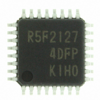
R5F21274SDFP#U0 Renesas Electronics America, R5F21274SDFP#U0 Datasheet - Page 231

R5F21274SDFP#U0
Manufacturer Part Number
R5F21274SDFP#U0
Description
IC R8C/27 MCU FLASH 32LQFP
Manufacturer
Renesas Electronics America
Series
R8C/2x/27r
Datasheet
1.R5F21272SDFPU0.pdf
(487 pages)
Specifications of R5F21274SDFP#U0
Core Processor
R8C
Core Size
16/32-Bit
Speed
20MHz
Connectivity
I²C, LIN, SIO, SSU, UART/USART
Peripherals
LED, POR, Voltage Detect, WDT
Number Of I /o
25
Program Memory Size
16KB (16K x 8)
Program Memory Type
FLASH
Ram Size
1K x 8
Voltage - Supply (vcc/vdd)
2.2 V ~ 5.5 V
Data Converters
A/D 12x10b
Oscillator Type
Internal
Operating Temperature
-40°C ~ 85°C
Package / Case
32-LQFP
For Use With
R0K521276S000BE - KIT DEV RSK-R8C/26-29R0E521000EPB00 - PROBE EMULATOR FOR PC7501
Lead Free Status / RoHS Status
Lead free / RoHS Compliant
Eeprom Size
-
Available stocks
Company
Part Number
Manufacturer
Quantity
Price
Part Number:
R5F21274SDFP#U0R5F21274SDFP#V2
Manufacturer:
Renesas Electronics America
Quantity:
10 000
- Current page: 231 of 487
- Download datasheet (5Mb)
R8C/26 Group, R8C/27 Group
Rev.2.10
REJ09B0278-0210
Figure 14.52
Table 14.21
j = A, B, C, or D
BFC, BFD: Bits in TRCMR register
NOTE:
TRCGRA
TRCGRB
TRCGRC
TRCGRD
TRCGRC
TRCGRD
Timer RC Control Register 1
b7 b6 b5 b4
j = B, C or D
NOTES:
Register
1. The output level does not change even when a compare match occurs if the TRCGRA register value (PWM
1.
2. If the pin function is set for w aveform output (refer to Table 7.15, Table 7.16, Tables 7.26 to 7.29, and Tables
period) is the same as the TRCGRB, TRCGRC, or TRCGRD register value.
Set to these bits w hen the TSTART bit in the TRCMR register is set to 0 (count stops).
7.37 to 7.40), the initial output level is output w hen the TRCCR1 register is set.
Sep 26, 2008
b3 b2
−
−
BFC = 0
BFD = 0
BFC = 1
BFD = 1
TRCCR1 Register in PWM Mode
Functions of TRCGRj Register in PWM Mode
b1 b0
Setting
Bit Symbol
TRCCR1
Symbol
CCLR
TCK0
TCK1
TCK2
TOA
TOB
TOC
TOD
Page 212 of 453
General register. Set the PWM period.
General register. Set the PWM output change point.
General register. Set the PWM output change point.
Buffer register. Set the next PWM period. (Refer to 14.3.3.2
Buffer Operation .)
Buffer register. Set the next PWM output change point. (Refer to
14.3.3.2 Buffer Operation .)
TRCIOA output level select bit
TRCIOB output level select bit
TRCIOC output level select bit
TRCIOD output level select bit
Count source select bits
TRC counter clear select bit
Address
Bit Name
0121h
Register Function
(1)
(1, 2)
(1, 2)
(1, 2)
(1)
b6 b5 b4
0 0 0 : f1
0 0 1 : f2
0 1 0 : f4
0 1 1 : f8
1 0 0 : f32
1 0 1 : TRCCLK input rising edge
1 1 0 : fOCO40M
1 1 1 : Do not set.
Disabled in PWM mode
0 : Active level “H”
1 : Active level “L”
0 : Disable clear (free-running operation)
1 : Clear by compare match in the
(Initial output “L”
“H” output by compare match in
the TRCGRj register
“L” output by compare match in
the TRCGRA register
(Initial output “H”
“L” output by compare match in
the TRCGRj register
“H” output by compare match in
the TRCGRA register
TRCGRA register
After Reset
Function
00h
TRCIOB
TRCIOC
−
TRCIOD
−
TRCIOB
PWM Output Pin
14. Timers
RW
RW
RW
RW
RW
RW
RW
RW
RW
Related parts for R5F21274SDFP#U0
Image
Part Number
Description
Manufacturer
Datasheet
Request
R

Part Number:
Description:
KIT STARTER FOR M16C/29
Manufacturer:
Renesas Electronics America
Datasheet:

Part Number:
Description:
KIT STARTER FOR R8C/2D
Manufacturer:
Renesas Electronics America
Datasheet:

Part Number:
Description:
R0K33062P STARTER KIT
Manufacturer:
Renesas Electronics America
Datasheet:

Part Number:
Description:
KIT STARTER FOR R8C/23 E8A
Manufacturer:
Renesas Electronics America
Datasheet:

Part Number:
Description:
KIT STARTER FOR R8C/25
Manufacturer:
Renesas Electronics America
Datasheet:

Part Number:
Description:
KIT STARTER H8S2456 SHARPE DSPLY
Manufacturer:
Renesas Electronics America
Datasheet:

Part Number:
Description:
KIT STARTER FOR R8C38C
Manufacturer:
Renesas Electronics America
Datasheet:

Part Number:
Description:
KIT STARTER FOR R8C35C
Manufacturer:
Renesas Electronics America
Datasheet:

Part Number:
Description:
KIT STARTER FOR R8CL3AC+LCD APPS
Manufacturer:
Renesas Electronics America
Datasheet:

Part Number:
Description:
KIT STARTER FOR RX610
Manufacturer:
Renesas Electronics America
Datasheet:

Part Number:
Description:
KIT STARTER FOR R32C/118
Manufacturer:
Renesas Electronics America
Datasheet:

Part Number:
Description:
KIT DEV RSK-R8C/26-29
Manufacturer:
Renesas Electronics America
Datasheet:

Part Number:
Description:
KIT STARTER FOR SH7124
Manufacturer:
Renesas Electronics America
Datasheet:

Part Number:
Description:
KIT STARTER FOR H8SX/1622
Manufacturer:
Renesas Electronics America
Datasheet:

Part Number:
Description:
KIT DEV FOR SH7203
Manufacturer:
Renesas Electronics America
Datasheet:


