R5F21274SDFP#U0 Renesas Electronics America, R5F21274SDFP#U0 Datasheet - Page 333
R5F21274SDFP#U0
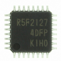
Manufacturer Part Number
R5F21274SDFP#U0
Description
IC R8C/27 MCU FLASH 32LQFP
Manufacturer
Renesas Electronics America
Series
R8C/2x/27r
Datasheet
1.R5F21272SDFPU0.pdf
(487 pages)
Specifications of R5F21274SDFP#U0
Core Processor
R8C
Core Size
16/32-Bit
Speed
20MHz
Connectivity
I²C, LIN, SIO, SSU, UART/USART
Peripherals
LED, POR, Voltage Detect, WDT
Number Of I /o
25
Program Memory Size
16KB (16K x 8)
Program Memory Type
FLASH
Ram Size
1K x 8
Voltage - Supply (vcc/vdd)
2.2 V ~ 5.5 V
Data Converters
A/D 12x10b
Oscillator Type
Internal
Operating Temperature
-40°C ~ 85°C
Package / Case
32-LQFP
For Use With
R0K521276S000BE - KIT DEV RSK-R8C/26-29R0E521000EPB00 - PROBE EMULATOR FOR PC7501
Lead Free Status / RoHS Status
Lead free / RoHS Compliant
Eeprom Size
-
Available stocks
Company
Part Number
Manufacturer
Quantity
Price

Part Number:
R5F21274SDFP#U0R5F21274SDFP#V2
Manufacturer:
Renesas Electronics America
Quantity:
10 000


R8C/26 Group, R8C/27 Group
Rev.2.10
REJ09B0278-0210
Figure 16.41
16.3.4.2
ICDRT register
ICDRS register
ICCR1 register
ICSR register
by program
In transmit mode, transmit data is output from the SDA pin in synchronization with the falling edge of the
transfer clock. The transfer clock is output when the MST bit in the ICCR1 register is set to 1 and input when
the MST bit is set to 0.
Figure 16.41 shows the Operating Timing in Transmit Mode (Clock Synchronous Serial Mode).
The transmit procedure and operation in transmit mode are as follows.
Processing
TDRE bit in
TRS bit in
(1) Set the ICE bit in the ICCR1 register to 1 (transfer operation enabled). Set bits CKS0 to CKS3 in the
(2) The TDRE bit in the ICSR register is set to 1 by selecting transmit mode after setting the TRS bit in the
(3) Data is transferred from registers ICDRT to ICDRS and the TDRE bit is automatically set to 1 by
(output)
Sep 26, 2008
SDA
SCL
ICCR1 register and set the MST bit (initial setting).
ICCR1 register to 1.
writing transmit data to the ICDRT register after confirming that the TDRE bit is set to 1. Continuous
transmission is enabled by writing data to the ICDRT register every time the TDRE bit is set to 1. When
switching from transmit to receive mode, set the TRS bit to 0 while the TDRE bit is set to 1.
(2) Set TRS bit to 1
Transmit Operation
Operating Timing in Transmit Mode (Clock Synchronous Serial Mode)
1
0
1
0
(3) Data write to
ICDRT register
Page 314 of 453
Data 1
b0
Data 1
1
b1
(3) Data write to
2
ICDRT register
b6
Data 2
7
b7
8
b0
Data 2
1
16. Clock Synchronous Serial Interface
(3) Data write to
b6
ICDRT register
7
b7
8
(3) Data write to
Data 3
Data 3
ICDRT register
b0
1
Related parts for R5F21274SDFP#U0
Image
Part Number
Description
Manufacturer
Datasheet
Request
R

Part Number:
Description:
KIT STARTER FOR M16C/29
Manufacturer:
Renesas Electronics America
Datasheet:

Part Number:
Description:
KIT STARTER FOR R8C/2D
Manufacturer:
Renesas Electronics America
Datasheet:

Part Number:
Description:
R0K33062P STARTER KIT
Manufacturer:
Renesas Electronics America
Datasheet:

Part Number:
Description:
KIT STARTER FOR R8C/23 E8A
Manufacturer:
Renesas Electronics America
Datasheet:

Part Number:
Description:
KIT STARTER FOR R8C/25
Manufacturer:
Renesas Electronics America
Datasheet:

Part Number:
Description:
KIT STARTER H8S2456 SHARPE DSPLY
Manufacturer:
Renesas Electronics America
Datasheet:

Part Number:
Description:
KIT STARTER FOR R8C38C
Manufacturer:
Renesas Electronics America
Datasheet:

Part Number:
Description:
KIT STARTER FOR R8C35C
Manufacturer:
Renesas Electronics America
Datasheet:

Part Number:
Description:
KIT STARTER FOR R8CL3AC+LCD APPS
Manufacturer:
Renesas Electronics America
Datasheet:
Part Number:
Description:
KIT STARTER FOR RX610
Manufacturer:
Renesas Electronics America
Datasheet:

Part Number:
Description:
KIT STARTER FOR R32C/118
Manufacturer:
Renesas Electronics America
Datasheet:

Part Number:
Description:
KIT DEV RSK-R8C/26-29
Manufacturer:
Renesas Electronics America
Datasheet:

Part Number:
Description:
KIT STARTER FOR SH7124
Manufacturer:
Renesas Electronics America
Datasheet:

Part Number:
Description:
KIT STARTER FOR H8SX/1622
Manufacturer:
Renesas Electronics America
Datasheet:

Part Number:
Description:
KIT DEV FOR SH7203
Manufacturer:
Renesas Electronics America
Datasheet: