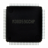
M38D59GCHP#U0 Renesas Electronics America, M38D59GCHP#U0 Datasheet - Page 138

M38D59GCHP#U0
Manufacturer Part Number
M38D59GCHP#U0
Description
IC 740/38D5 MCU QZ-ROM 80LQFP
Manufacturer
Renesas Electronics America
Series
740/38000r
Datasheet
1.M38D58G8FPU0.pdf
(144 pages)
Specifications of M38D59GCHP#U0
Core Processor
740
Core Size
8-Bit
Speed
12.5MHz
Connectivity
SIO, UART/USART
Peripherals
LCD, LED, PWM, WDT
Number Of I /o
59
Program Memory Size
48KB (48K x 8)
Program Memory Type
QzROM
Ram Size
2K x 8
Voltage - Supply (vcc/vdd)
1.8 V ~ 5.5 V
Data Converters
A/D 8x10b
Oscillator Type
Internal
Operating Temperature
-20°C ~ 85°C
Package / Case
80-LQFP
Lead Free Status / RoHS Status
Lead free / RoHS Compliant
Eeprom Size
-
Available stocks
Company
Part Number
Manufacturer
Quantity
Price
Rev.
2.00
2.01
2.02
2.03
REVISION HISTORY
Aug 31, 2006
Mar 24, 2006
Jan 23, 2006
Jul 10, 2006
Date
64 to 67
Page
71
73
74
75
76
77
81
17
52
53
58
59
60
71
73
76
15
22
23
29
32
33
35
43
52
53
58
61
76
23
1
4
4
7
Table 14 Recommended operating conditions
- Vcc (Power source voltage) and Note revised.
- V
Table 16 Recommended operating conditions: all revised, Power source voltage
graph added.
Table 17 Electrical characteristics: ROSC → f(OCO)
Table 18 Electrical characteristics: Icc revised.
Table 19 A/D converter recommended operating condition revised.
Table 20 A/D converter characteristics: test conditions revised.
AD Power source voltage graph added.
Table 21 Timing requirements 1: t
PACKAGE OUTLINE revised.
FEATURES: Power source voltage revised.
Performance overview: Oscillation frequency and Power source voltage revised.
Table 7 Related SFRs of port P7 revised.
Fig. 46: Address revised.
Fig. 50: Note 1 revised.
(1)Stop mode: Description revised.
Fig. 59 φ
Fig. 60 State transitions of system clock: Note 3 revised.
Table 14 : Vcc (Power source voltage) and Note 3 revised.
Table 16: Power source voltage (Main clock X
Table 20 Description of f(OCO) and Note revised.
Fig. 11: Register names of ROM correction addresses 1 and 2 revised.
Termination of unused pins
Table 8
• Termination 1 (recommended) : Delete (recommended).
• Termination 1 to 3 of P7
X
X
Fig. 26: (TXCON1 bit 5 = “1”) → (TXCON1 bit 5 = “0”)
X
Fig. 38:
Fig. 47: Border line in ROM area : revised.
Fig. 49: On chip oscillator → On chip oscillator/4
Fig. 50: b5 and b7 revised.
Frequency Control : Description added.
Table 12: Function of V
Fig. 63 to Fig. 66: Revised and added.
Table 17: Parameter of I
Table 1: Main clock and Sub-clock generating circuit : “feedback resistor”
Table 3: AV
Table 8: P4
CIN
CIN
CIN
IH
, V
is selected as Timer 1, 2 count source : sentence is revised.
is selected as Timer X count source : sentence is revised.
is selected as Timer Y count source : sentence is revised.
IL
φ SOURCE
SOURCE
eliminated.
P4
(RESET) revised.
SS
1
2
/TxD : input port → output port
/S
: GND → Analog power source
CLK1
added.
clock added.
: output port → input port
(2/7)
REF
IH
0
/C
and I
38D5 Group Data Sheet
and AV
1
/INT
Description
I/O ports : Description added.
IC
c
01
added.
(X
SS
and P7
IN
Summary
revised.
), t
wH
(X
1
/C
IN
IN
2
), t
/INT
frequency) graph added.
wL
11
(X
: revised.
IN
) revised and Note added.


