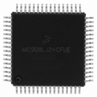
MC908LJ24CFUE Freescale Semiconductor, MC908LJ24CFUE Datasheet - Page 188

MC908LJ24CFUE
Manufacturer Part Number
MC908LJ24CFUE
Description
IC MCU 24K FLASH 8MHZ SPI 64-QFP
Manufacturer
Freescale Semiconductor
Series
HC08r
Datasheet
1.MC908LK24CFUE.pdf
(464 pages)
Specifications of MC908LJ24CFUE
Core Processor
HC08
Core Size
8-Bit
Speed
8MHz
Connectivity
I²C, IRSCI, SPI
Peripherals
LCD, LVD, POR, PWM
Number Of I /o
40
Program Memory Size
24KB (24K x 8)
Program Memory Type
FLASH
Ram Size
768 x 8
Voltage - Supply (vcc/vdd)
3 V ~ 5.5 V
Data Converters
A/D 6x10b
Oscillator Type
Internal
Operating Temperature
-40°C ~ 85°C
Package / Case
64-QFP
Processor Series
HC08LJ
Core
HC08
Data Bus Width
8 bit
Data Ram Size
768 B
Interface Type
SCI/SPI
Maximum Clock Frequency
8 MHz
Number Of Programmable I/os
48
Number Of Timers
4
Operating Supply Voltage
3.3 V, 5 V
Maximum Operating Temperature
+ 85 C
Mounting Style
SMD/SMT
Development Tools By Supplier
FSICEBASE, M68EML08LJLKE, ZK-HC08LX-A, M68CBL05CE
Minimum Operating Temperature
- 40 C
On-chip Adc
6-ch x 10-bit
Controller Family/series
HC08
No. Of I/o's
40
Ram Memory Size
768Byte
Cpu Speed
8MHz
No. Of Timers
2
Embedded Interface Type
I2C, SCI, SPI
Rohs Compliant
Yes
Lead Free Status / RoHS Status
Lead free / RoHS Compliant
Eeprom Size
-
Lead Free Status / Rohs Status
Lead free / RoHS Compliant
Available stocks
Company
Part Number
Manufacturer
Quantity
Price
Company:
Part Number:
MC908LJ24CFUE
Manufacturer:
Freescale Semiconductor
Quantity:
10 000
Company:
Part Number:
MC908LJ24CFUER
Manufacturer:
Freescale Semiconductor
Quantity:
10 000
- Current page: 188 of 464
- Download datasheet (5Mb)
Monitor ROM (MON)
10.6.7 EE_WRITE
Data Sheet
188
EE_WRITE is used to write a set of data from the data array to FLASH.
The start location of the FLASH to be programmed is specified by the
address ADDRH:ADDRL and the number of bytes in the data array is
specified by DATASIZE. The minimum number of bytes that can be
programmed in one routine call is 2 bytes, the maximum is 15 bytes.
ADDRH:ADDRL must always be the start of boundary address (the page
start address: $XX00 or $0080) and DATASIZE must be the same size
when accessing the same page.
In some applications, the user may want to repeatedly store and read a
set of data from an area of non-volatile memory. This is easily possible
when using an EEPROM array. As the write and erase operations can
be executed on a byte basis. For FLASH memory, the minimum erase
size is the page — 128 bytes per page for MC68HC908LJ24. If the data
array size is less than the page size, writing and erasing to the same
page cannot fully utilize the page. Unused locations in the page will be
wasted. The EE_WRITE routine is designed to emulate the properties
similar to the EEPROM. Allowing a more efficient use of the FLASH page
for data storage.
Notes:
Routine Name
Routine Description
Calling Address
Stack Used
Data Block Format
1. The minimum data size is 2 bytes. The maximum data size is 15 bytes.
2. The start address must be a page boundary start address, e.g. $xx00 or $xx80.
Monitor ROM (MON)
Table 10-17. EE_WRITE Routine
EE_WRITE
Emulated EEPROM write. Data size ranges from 2 to 15
bytes at a time.
$FC00
17 bytes
Bus speed (BUS_SPD)
Data size (DATASIZE)
Starting address (ADDRH)
Starting address (ADDRL)
Data 1
Data N
:
(1)
MC68HC908LJ24/LK24 — Rev. 2.1
(1)
(2)
Freescale Semiconductor
Related parts for MC908LJ24CFUE
Image
Part Number
Description
Manufacturer
Datasheet
Request
R
Part Number:
Description:
Manufacturer:
Freescale Semiconductor, Inc
Datasheet:
Part Number:
Description:
Manufacturer:
Freescale Semiconductor, Inc
Datasheet:
Part Number:
Description:
Manufacturer:
Freescale Semiconductor, Inc
Datasheet:
Part Number:
Description:
Manufacturer:
Freescale Semiconductor, Inc
Datasheet:
Part Number:
Description:
Manufacturer:
Freescale Semiconductor, Inc
Datasheet:
Part Number:
Description:
Manufacturer:
Freescale Semiconductor, Inc
Datasheet:
Part Number:
Description:
Manufacturer:
Freescale Semiconductor, Inc
Datasheet:
Part Number:
Description:
Manufacturer:
Freescale Semiconductor, Inc
Datasheet:
Part Number:
Description:
Manufacturer:
Freescale Semiconductor, Inc
Datasheet:
Part Number:
Description:
Manufacturer:
Freescale Semiconductor, Inc
Datasheet:
Part Number:
Description:
Manufacturer:
Freescale Semiconductor, Inc
Datasheet:
Part Number:
Description:
Manufacturer:
Freescale Semiconductor, Inc
Datasheet:
Part Number:
Description:
Manufacturer:
Freescale Semiconductor, Inc
Datasheet:
Part Number:
Description:
Manufacturer:
Freescale Semiconductor, Inc
Datasheet:
Part Number:
Description:
Manufacturer:
Freescale Semiconductor, Inc
Datasheet:


