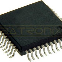
MC68HC705C9ACFBE Freescale Semiconductor, MC68HC705C9ACFBE Datasheet - Page 18

MC68HC705C9ACFBE
Manufacturer Part Number
MC68HC705C9ACFBE
Description
IC MCU 8BIT 44-QFP
Manufacturer
Freescale Semiconductor
Series
HC05r
Datasheet
1.MC705C9ACPE.pdf
(118 pages)
Specifications of MC68HC705C9ACFBE
Core Processor
HC05
Core Size
8-Bit
Speed
2.1MHz
Connectivity
SCI, SPI
Peripherals
POR, WDT
Number Of I /o
24
Program Memory Size
16KB (16K x 8)
Program Memory Type
OTP
Ram Size
352 x 8
Voltage - Supply (vcc/vdd)
3 V ~ 5.5 V
Oscillator Type
Internal
Operating Temperature
-40°C ~ 85°C
Package / Case
44-QFP
Processor Series
HC705C
Core
HC05
Data Bus Width
8 bit
Data Ram Size
352 B
Interface Type
SCI, SPI
Maximum Clock Frequency
2.1 MHz
Number Of Programmable I/os
31
Number Of Timers
1
Maximum Operating Temperature
+ 85 C
Mounting Style
SMD/SMT
Minimum Operating Temperature
- 40 C
On-chip Adc
8 bit
Package
44PQFP
Family Name
HC05
Maximum Speed
2.1 MHz
Operating Supply Voltage
3.3|5 V
Lead Free Status / RoHS Status
Lead free / RoHS Compliant
Eeprom Size
-
Data Converters
-
Lead Free Status / Rohs Status
Details
Available stocks
Company
Part Number
Manufacturer
Quantity
Price
Company:
Part Number:
MC68HC705C9ACFBE
Manufacturer:
FREESCALE
Quantity:
1 827
Company:
Part Number:
MC68HC705C9ACFBE
Manufacturer:
Freescale Semiconductor
Quantity:
10 000
General Description
1.5 Software-Programmable Options (MC68HC05C9A Mode Only)
The C9A option register (OR), shown in
register contains the programmable bits for the following options:
This register must be written to by user software during operation of the microcontroller.
RAM0 — Random Access Memory Control Bit 0
RAM1— Random Access Memory Control Bit 1
IRQ — Interrupt Request Bit
18
•
•
This read/write bit selects between RAM or EPROM in location $0020 to $004F. This bit can be read
or written at any time.
This read/write bit selects between RAM or EPROM in location $0100 to $017F. This bit can be read
or written at any time.
This bit selects between an edge-triggered only or edge- and level- triggered external interrupt pin.
This bit is set by reset, but can be cleared by software. This bit can be written only once.
1 = RAM selected
0 = EPROM selected
1 = RAM selected
0 = EPROM selected
1 = Edge and level interrupt option selected
0 = Edge-only interrupt option selected
Map two different areas of memory between RAM and EPROM, one of 48 bytes and one of 128
bytes
Edge-triggered only or edge- and level-triggered external interrupt (IRQ pin and any port B pin
configured for interrupt)
$3FDF
Reset:
Read:
Write:
RAM0
Bit 7
0
MC68HC05C9A Advance Information Data Sheet, Rev. 4.1
= Unimplemented
RAM1
6
0
Figure 1-4. C9A Option Register
Figure
5
0
1-4, is enabled only if configured in C9A mode. This
4
0
3
0
2
0
IRQ
1
1
Freescale Semiconductor
Bit 0
0


