MC68HC705C9ACFBE Freescale Semiconductor, MC68HC705C9ACFBE Datasheet - Page 72
MC68HC705C9ACFBE
Manufacturer Part Number
MC68HC705C9ACFBE
Description
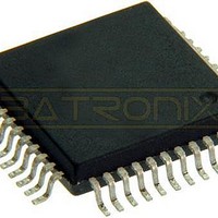
IC MCU 8BIT 44-QFP
Manufacturer
Freescale Semiconductor
Series
HC05r
Datasheet
1.MC705C9ACPE.pdf
(118 pages)
Specifications of MC68HC705C9ACFBE
Core Processor
HC05
Core Size
8-Bit
Speed
2.1MHz
Connectivity
SCI, SPI
Peripherals
POR, WDT
Number Of I /o
24
Program Memory Size
16KB (16K x 8)
Program Memory Type
OTP
Ram Size
352 x 8
Voltage - Supply (vcc/vdd)
3 V ~ 5.5 V
Oscillator Type
Internal
Operating Temperature
-40°C ~ 85°C
Package / Case
44-QFP
Processor Series
HC705C
Core
HC05
Data Bus Width
8 bit
Data Ram Size
352 B
Interface Type
SCI, SPI
Maximum Clock Frequency
2.1 MHz
Number Of Programmable I/os
31
Number Of Timers
1
Maximum Operating Temperature
+ 85 C
Mounting Style
SMD/SMT
Minimum Operating Temperature
- 40 C
On-chip Adc
8 bit
Package
44PQFP
Family Name
HC05
Maximum Speed
2.1 MHz
Operating Supply Voltage
3.3|5 V
Lead Free Status / RoHS Status
Lead free / RoHS Compliant
Eeprom Size
-
Data Converters
-
Lead Free Status / Rohs Status
Details
Available stocks
Company
Part Number
Manufacturer
Quantity
Price
Company:

Part Number:
MC68HC705C9ACFBE
Manufacturer:
FREESCALE
Quantity:
1 827
Company:
Part Number:
MC68HC705C9ACFBE
Manufacturer:
Freescale Semiconductor
Quantity:
10 000


Serial Peripheral Interface (SPI)
10.3.1 Master In Slave Out (MISO)
The MISO line is configured as an input in a master device and as an output in a slave device. It is one
of the two lines that transfer serial data in one direction, with the most significant bit sent first. The MISO
line of a slave device is placed in the high-impedance state if the slave is not selected.
10.3.2 Master Out Slave In (MOSI)
The MOSI line is configured as an output in a master device and as an input in a slave device. It is one
of the two lines that transfer serial data in one direction with the most significant bit sent first.
10.3.3 Serial Clock (SCK)
The master clock is used to synchronize data movement both in and out of the device through its MOSI
and MISO lines. The master and slave devices are capable of exchanging a byte of information during a
sequence of eight clock cycles. Since SCK is generated by the master device, this line becomes an input
on a slave device.
As shown in
and CPHA in the serial peripheral control register (SPCR). Both master and slave devices must operate
with the same timing. The master device always places data on the MOSI line a half cycle before the clock
edge (SCK), in order for the slave device to latch the data.
Two bits (SPR0 and SPR1) in the SPCR of the master device select the clock rate. In a slave device,
SPR0 and SPR1 have no effect on the operation of the SPI.
10.3.4 Slave Select (SS)
The slave select (SS) input line is used to select a slave device. It has to be low prior to data transactions
and must stay low for the duration of the transaction.The SS line on the master must be tied high. In
master mode, if the SS pin is pulled low during a transmission, a mode fault error flag (MODF) is set in
72
Figure
MISO/MOSI
SCK
SCK
SCK
SCK
SS
10-1, four possible timing relationships may be chosen by using control bits CPOL
MC68HC05C9A Advance Information Data Sheet, Rev. 4.1
MSB
Figure 10-1. Data Clock Timing Diagram
6
INTERNAL STROBE FOR DATA CAPTURE (ALL MODES)
5
4
3
2
1
0
Freescale Semiconductor
CPOL = 0
CPHA = 0
CPOL = 0
CPHA = 1
CPOL = 1
CPHA = 0
CPOL = 1
CPHA = 1
Related parts for MC68HC705C9ACFBE
Image
Part Number
Description
Manufacturer
Datasheet
Request
R

Part Number:
Description:
APPENDIX A ELECTRICAL CHARACTERISTICS
Manufacturer:
FREESCALE [Freescale Semiconductor, Inc]
Datasheet:

Part Number:
Description:
Manufacturer:
Freescale Semiconductor, Inc
Datasheet:
Part Number:
Description:
Manufacturer:
Freescale Semiconductor, Inc
Datasheet:
Part Number:
Description:
Manufacturer:
Freescale Semiconductor, Inc
Datasheet:
Part Number:
Description:
Manufacturer:
Freescale Semiconductor, Inc
Datasheet:
Part Number:
Description:
Manufacturer:
Freescale Semiconductor, Inc
Datasheet:
Part Number:
Description:
Manufacturer:
Freescale Semiconductor, Inc
Datasheet:
Part Number:
Description:
Manufacturer:
Freescale Semiconductor, Inc
Datasheet:
Part Number:
Description:
Manufacturer:
Freescale Semiconductor, Inc
Datasheet:
Part Number:
Description:
Manufacturer:
Freescale Semiconductor, Inc
Datasheet:
Part Number:
Description:
Manufacturer:
Freescale Semiconductor, Inc
Datasheet:
Part Number:
Description:
Manufacturer:
Freescale Semiconductor, Inc
Datasheet:
Part Number:
Description:
Manufacturer:
Freescale Semiconductor, Inc
Datasheet:
Part Number:
Description:
Manufacturer:
Freescale Semiconductor, Inc
Datasheet:
Part Number:
Description:
Manufacturer:
Freescale Semiconductor, Inc
Datasheet: