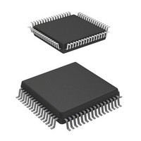
HD64F3644H Renesas Electronics America, HD64F3644H Datasheet - Page 68

HD64F3644H
Manufacturer Part Number
HD64F3644H
Description
IC H8 MCU FLASH 32K 64-QFP
Manufacturer
Renesas Electronics America
Series
H8® H8/300Lr
Datasheet
1.HD64F3644HV.pdf
(551 pages)
Specifications of HD64F3644H
Core Processor
H8/300L
Core Size
8-Bit
Speed
8MHz
Connectivity
SCI
Peripherals
PWM, WDT
Number Of I /o
53
Program Memory Size
32KB (32K x 8)
Program Memory Type
FLASH
Ram Size
1K x 8
Voltage - Supply (vcc/vdd)
2.7 V ~ 5.5 V
Data Converters
A/D 8x8b
Oscillator Type
Internal
Operating Temperature
-20°C ~ 75°C
Package / Case
64-QFP
Package
64PQFP
Family Name
H8
Maximum Speed
8 MHz
Operating Supply Voltage
3.3|5 V
Data Bus Width
8 Bit
Number Of Programmable I/os
45
Interface Type
SCI
On-chip Adc
8-chx8-bit
Number Of Timers
4
Lead Free Status / RoHS Status
Contains lead / RoHS non-compliant
Eeprom Size
-
Available stocks
Company
Part Number
Manufacturer
Quantity
Price
Company:
Part Number:
HD64F3644H
Manufacturer:
HITACHI
Quantity:
490
Company:
Part Number:
HD64F3644H
Manufacturer:
Renesas Electronics America
Quantity:
10 000
Part Number:
HD64F3644H
Manufacturer:
HD
Quantity:
20 000
Company:
Part Number:
HD64F3644HV
Manufacturer:
Renesas
Quantity:
600
Company:
Part Number:
HD64F3644HV
Manufacturer:
Renesas Electronics America
Quantity:
10 000
Part Number:
HD64F3644HV
Manufacturer:
RENESAS/瑞萨
Quantity:
20 000
Part Number:
HD64F3644HV/H83644
Manufacturer:
RENESAS/瑞萨
Quantity:
20 000
- Current page: 68 of 551
- Download datasheet (4Mb)
Section 2 CPU
Three-State Access to On-Chip Peripheral Modules: Figure 2.13 shows the operation timing in
the case of three-state access to an on-chip peripheral module.
2.7
2.7.1
There are four CPU states: the reset state, program execution state, program halt state, and
exception-handling state. The program execution state includes active (high-speed or medium-
speed) mode and subactive mode. In the program halt state there are a sleep (high-speed or
medium-speed) mode, standby mode, watch mode, and sub-sleep mode. These states are shown in
figure 2.14. Figure 2.15 shows the state transitions.
Rev. 6.00 Sep 12, 2006 page 46 of 526
REJ09B0326-0600
Internal
address bus
Internal
read signal
Internal
data bus
(read access)
Internal
write signal
Internal
data bus
(write access)
or
SUB
CPU States
Overview
Figure 2.13 On-Chip Peripheral Module Access Cycle (3-State Access)
T
1
state
Address
Bus cycle
T
2
state
Read data
Write data
T
3
state
Related parts for HD64F3644H
Image
Part Number
Description
Manufacturer
Datasheet
Request
R

Part Number:
Description:
(HD64 Series) Hitachi Single-Chip Microcomputer
Manufacturer:
Hitachi Semiconductor
Datasheet:

Part Number:
Description:
KIT STARTER FOR M16C/29
Manufacturer:
Renesas Electronics America
Datasheet:

Part Number:
Description:
KIT STARTER FOR R8C/2D
Manufacturer:
Renesas Electronics America
Datasheet:

Part Number:
Description:
R0K33062P STARTER KIT
Manufacturer:
Renesas Electronics America
Datasheet:

Part Number:
Description:
KIT STARTER FOR R8C/23 E8A
Manufacturer:
Renesas Electronics America
Datasheet:

Part Number:
Description:
KIT STARTER FOR R8C/25
Manufacturer:
Renesas Electronics America
Datasheet:

Part Number:
Description:
KIT STARTER H8S2456 SHARPE DSPLY
Manufacturer:
Renesas Electronics America
Datasheet:

Part Number:
Description:
KIT STARTER FOR R8C38C
Manufacturer:
Renesas Electronics America
Datasheet:

Part Number:
Description:
KIT STARTER FOR R8C35C
Manufacturer:
Renesas Electronics America
Datasheet:

Part Number:
Description:
KIT STARTER FOR R8CL3AC+LCD APPS
Manufacturer:
Renesas Electronics America
Datasheet:

Part Number:
Description:
KIT STARTER FOR RX610
Manufacturer:
Renesas Electronics America
Datasheet:

Part Number:
Description:
KIT STARTER FOR R32C/118
Manufacturer:
Renesas Electronics America
Datasheet:

Part Number:
Description:
KIT DEV RSK-R8C/26-29
Manufacturer:
Renesas Electronics America
Datasheet:

Part Number:
Description:
KIT STARTER FOR SH7124
Manufacturer:
Renesas Electronics America
Datasheet:

Part Number:
Description:
KIT STARTER FOR H8SX/1622
Manufacturer:
Renesas Electronics America
Datasheet:


