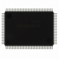
M30626SPFP#U5C Renesas Electronics America, M30626SPFP#U5C Datasheet - Page 212

M30626SPFP#U5C
Manufacturer Part Number
M30626SPFP#U5C
Description
IC M16C/62P MCU ROMLESS 100QFP
Manufacturer
Renesas Electronics America
Series
M16C™ M16C/60r
Datasheet
1.M30620SPGPU3C.pdf
(423 pages)
Specifications of M30626SPFP#U5C
Core Processor
M16C/60
Core Size
16-Bit
Speed
24MHz
Connectivity
I²C, IEBus, UART/USART
Peripherals
DMA, WDT
Number Of I /o
50
Program Memory Type
ROMless
Ram Size
31K x 8
Voltage - Supply (vcc/vdd)
2.7 V ~ 5.5 V
Data Converters
A/D 26x10b; D/A 2x8b
Oscillator Type
Internal
Operating Temperature
-20°C ~ 85°C
Package / Case
100-QFP
For Use With
867-1000 - KIT QUICK START RENESAS 62PR0K33062PS001BE - R0K33062P STARTER KITR0K33062PS000BE - KIT EVAL STARTER FOR M16C/62PM3062PT3-CPE-3 - EMULATOR COMPACT M16C/62P/30P
Lead Free Status / RoHS Status
Lead free / RoHS Compliant
Eeprom Size
-
Program Memory Size
-
Available stocks
Company
Part Number
Manufacturer
Quantity
Price
Part Number:
M30626SPFP#U5CM30626SPFP#U3C
Manufacturer:
Renesas Electronics America
Quantity:
10 000
- Current page: 212 of 423
- Download datasheet (5Mb)
M16C/62P Group (M16C/62P, M16C/62PT)
Rev.2.41
REJ09B0185-0241
Figure 17.16
Figure 17.17
17.1.1.5
17.1.1.6
When the UiLCH bit in the UiC1 register (i = 0 to 2) = 1 (reverse), the data written to the UiTB register has its
logic reversed before being transmitted. Similarly, the received data has its logic reversed when read from the
UiRB register. Figure 17.16 shows Serial Data Logic Switching.
Use the CLKMD1 to CLKMD0 bits in the UCON register to select one of the two transfer clock output pins
(see Figure 17.17). This function can be used when the selected transfer clock for UART1 is an internal clock.
Jan 10, 2006
(1) When The UiLCH Bit in The UiC1 Register = 0 (No Reverse)
(2) When The UiLCH Bit = 1 (Reverse)
Serial Data Logic Switching Function
NOTES :
i = 0 to 2
Transfer Clock Output From Multiple Pins (UART1)
Transfer Clock Output from Multiple Pins
Serial Data Logic Switching
NOTES :
Microcomputer
Transfer Clock
Transfer Clock
(No Reverse)
1. This applies to the case where the CKDIR bit in the U1MR register= 0
1. This applies to the case where the CKPOL bit in the UiC0 register = 0
CLKS1 (P6_4)
TXD1 (P6_7)
CLK1 (P6_5)
(Reverse)
(internal clock) and the CLKMD1 bit in the UCON register = 1
(transfer clock output from multiple pins).
(transmit data output at the falling edge and the receive data taken
in at the rising edge of the transfer clock) and the UFORM bit = 0
(LSB first).
TXDi
TXDi
Page 195 of 390
“H”
“H”
“H”
“H”
“L”
“L”
“L”
“L”
D0
D0
D1
D1
Transfer enabled
when the CLKMD0
bit in the UCON
register = 0
IN
CLK
D2
D2
D3
D3
D4
D4
D5
D5
Transfer enabled
when the CLKMD0
bit = 1
D6
D6
IN
CLK
D7
D7
17. Serial Interface
Related parts for M30626SPFP#U5C
Image
Part Number
Description
Manufacturer
Datasheet
Request
R

Part Number:
Description:
KIT STARTER FOR M16C/29
Manufacturer:
Renesas Electronics America
Datasheet:

Part Number:
Description:
KIT STARTER FOR R8C/2D
Manufacturer:
Renesas Electronics America
Datasheet:

Part Number:
Description:
R0K33062P STARTER KIT
Manufacturer:
Renesas Electronics America
Datasheet:

Part Number:
Description:
KIT STARTER FOR R8C/23 E8A
Manufacturer:
Renesas Electronics America
Datasheet:

Part Number:
Description:
KIT STARTER FOR R8C/25
Manufacturer:
Renesas Electronics America
Datasheet:

Part Number:
Description:
KIT STARTER H8S2456 SHARPE DSPLY
Manufacturer:
Renesas Electronics America
Datasheet:

Part Number:
Description:
KIT STARTER FOR R8C38C
Manufacturer:
Renesas Electronics America
Datasheet:

Part Number:
Description:
KIT STARTER FOR R8C35C
Manufacturer:
Renesas Electronics America
Datasheet:

Part Number:
Description:
KIT STARTER FOR R8CL3AC+LCD APPS
Manufacturer:
Renesas Electronics America
Datasheet:

Part Number:
Description:
KIT STARTER FOR RX610
Manufacturer:
Renesas Electronics America
Datasheet:

Part Number:
Description:
KIT STARTER FOR R32C/118
Manufacturer:
Renesas Electronics America
Datasheet:

Part Number:
Description:
KIT DEV RSK-R8C/26-29
Manufacturer:
Renesas Electronics America
Datasheet:

Part Number:
Description:
KIT STARTER FOR SH7124
Manufacturer:
Renesas Electronics America
Datasheet:

Part Number:
Description:
KIT STARTER FOR H8SX/1622
Manufacturer:
Renesas Electronics America
Datasheet:

Part Number:
Description:
KIT DEV FOR SH7203
Manufacturer:
Renesas Electronics America
Datasheet:


