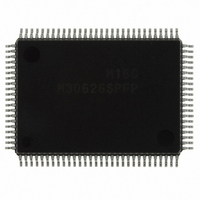
M30626SPFP#U5C Renesas Electronics America, M30626SPFP#U5C Datasheet - Page 280

M30626SPFP#U5C
Manufacturer Part Number
M30626SPFP#U5C
Description
IC M16C/62P MCU ROMLESS 100QFP
Manufacturer
Renesas Electronics America
Series
M16C™ M16C/60r
Datasheet
1.M30620SPGPU3C.pdf
(423 pages)
Specifications of M30626SPFP#U5C
Core Processor
M16C/60
Core Size
16-Bit
Speed
24MHz
Connectivity
I²C, IEBus, UART/USART
Peripherals
DMA, WDT
Number Of I /o
50
Program Memory Type
ROMless
Ram Size
31K x 8
Voltage - Supply (vcc/vdd)
2.7 V ~ 5.5 V
Data Converters
A/D 26x10b; D/A 2x8b
Oscillator Type
Internal
Operating Temperature
-20°C ~ 85°C
Package / Case
100-QFP
For Use With
867-1000 - KIT QUICK START RENESAS 62PR0K33062PS001BE - R0K33062P STARTER KITR0K33062PS000BE - KIT EVAL STARTER FOR M16C/62PM3062PT3-CPE-3 - EMULATOR COMPACT M16C/62P/30P
Lead Free Status / RoHS Status
Lead free / RoHS Compliant
Eeprom Size
-
Program Memory Size
-
Available stocks
Company
Part Number
Manufacturer
Quantity
Price
Part Number:
M30626SPFP#U5CM30626SPFP#U3C
Manufacturer:
Renesas Electronics America
Quantity:
10 000
- Current page: 280 of 423
- Download datasheet (5Mb)
M16C/62P Group (M16C/62P, M16C/62PT)
Rev.2.41
REJ09B0185-0241
Figure 21.8
Port P8 Register
Port Pi Register (i=0 to 7 and 9 to 13)
b7 b6 b5 b4
b7 b6 b5 b4
NOTES :
1.
2.
3.
Since P7_0 and P7_1 are N-channel open drain ports, the data is high-impedance.
During memory extension and microprocessor modes, the Pi register for the pins functioning as bus control pins (A0 to
A19, D0 to D15, CS0
To use ports P11 to P14, set the PU37 bit in the PUR3 register to “1” (enable). If this bit is set to “0” (disable), the P11 to
P14 registers are cleared to “0”.
Jan 10, 2006
b3 b2 b1 b0
b3 b2 b1 b0
Pi Registers
Bit Symbol
Bit Symbol
_____
P0 to P3
P4 to P7
P9 to P12
P13
P8_0
P8_1
P8_2
P8_3
P8_4
P8_5
P8_6
P8_7
Pi_0
Pi_1
Pi_2
Pi_3
Pi_4
Pi_5
Pi_6
Pi_7
Symbol
Page 263 of 390
Symbol
to CS3
P8
_____
, RD
Port P8_0 Bit
Port P8_1 Bit
Port P8_2 Bit
Port P8_3 Bit
Port P8_4 Bit
Port P8_5 Bit
Port P8_6 Bit
Port P8_7 Bit
Port Pi_0 Bit
Port Pi_1 Bit
Port Pi_2 Bit
Port Pi_3 Bit
Port Pi_4 Bit
Port Pi_5 Bit
Port Pi_6 Bit
Port Pi_7 Bit
___
, WRL
______
(2, 3)
Bit Name
03E0h, 03E1h, 03E4h, 03E5h
03E8h, 03E9h, 03ECh, 03EDh
03F1h, 03F4h, 03F5h, 03F8h
03F9h
/WR
Bit Name
___
, WRH
______
Address
/BHE
03F0h
_____
Address
, ALE, RDY
The pin level on any I/O port w hich is set for input mode
can be read by reading the corresponding bit in this
register.
The pin level on any I/O port w hich is set for output
mode can be controlled by w riting to the corresponding
bit in this register (except for P8_5)
0 : “L” level
1 : “H” level
The pin level on any I/O port w hich is set for input
mode can be read by reading the corresponding bit in
this register.
The pin level on any I/O port w hich is set for output
mode can be controlled by w riting to the
orresponding bit in this register
0 : “L” level
1 : “H” level
_____
(i = 0 to 7 and 9 to 13)
, HOLD
_______
(1)
, HLDA
_______
and BCLK) cannot be modified.
Function
Function
Indeterminate
After Reset
Indeterminate
Indeterminate
Indeterminate
Indeterminate
After Reset
21. Programmable I/O Ports
RW
RW
RW
RW
RW
RW
RW
RW
RW
RW
RW
RW
RW
RW
RW
RO
RW
RW
Related parts for M30626SPFP#U5C
Image
Part Number
Description
Manufacturer
Datasheet
Request
R

Part Number:
Description:
KIT STARTER FOR M16C/29
Manufacturer:
Renesas Electronics America
Datasheet:

Part Number:
Description:
KIT STARTER FOR R8C/2D
Manufacturer:
Renesas Electronics America
Datasheet:

Part Number:
Description:
R0K33062P STARTER KIT
Manufacturer:
Renesas Electronics America
Datasheet:

Part Number:
Description:
KIT STARTER FOR R8C/23 E8A
Manufacturer:
Renesas Electronics America
Datasheet:

Part Number:
Description:
KIT STARTER FOR R8C/25
Manufacturer:
Renesas Electronics America
Datasheet:

Part Number:
Description:
KIT STARTER H8S2456 SHARPE DSPLY
Manufacturer:
Renesas Electronics America
Datasheet:

Part Number:
Description:
KIT STARTER FOR R8C38C
Manufacturer:
Renesas Electronics America
Datasheet:

Part Number:
Description:
KIT STARTER FOR R8C35C
Manufacturer:
Renesas Electronics America
Datasheet:

Part Number:
Description:
KIT STARTER FOR R8CL3AC+LCD APPS
Manufacturer:
Renesas Electronics America
Datasheet:

Part Number:
Description:
KIT STARTER FOR RX610
Manufacturer:
Renesas Electronics America
Datasheet:

Part Number:
Description:
KIT STARTER FOR R32C/118
Manufacturer:
Renesas Electronics America
Datasheet:

Part Number:
Description:
KIT DEV RSK-R8C/26-29
Manufacturer:
Renesas Electronics America
Datasheet:

Part Number:
Description:
KIT STARTER FOR SH7124
Manufacturer:
Renesas Electronics America
Datasheet:

Part Number:
Description:
KIT STARTER FOR H8SX/1622
Manufacturer:
Renesas Electronics America
Datasheet:

Part Number:
Description:
KIT DEV FOR SH7203
Manufacturer:
Renesas Electronics America
Datasheet:


