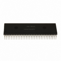
HD64F3644PV Renesas Electronics America, HD64F3644PV Datasheet - Page 143

HD64F3644PV
Manufacturer Part Number
HD64F3644PV
Description
IC H8/3644 MCU FLASH 32K 64SDIP
Manufacturer
Renesas Electronics America
Series
H8® H8/300Lr
Datasheet
1.HD64F3644HV.pdf
(551 pages)
Specifications of HD64F3644PV
Core Processor
H8/300L
Core Size
8-Bit
Speed
8MHz
Connectivity
SCI
Peripherals
PWM, WDT
Number Of I /o
53
Program Memory Size
32KB (32K x 8)
Program Memory Type
FLASH
Ram Size
1K x 8
Voltage - Supply (vcc/vdd)
2.7 V ~ 5.5 V
Data Converters
A/D 8x8b
Oscillator Type
Internal
Operating Temperature
-20°C ~ 75°C
Package / Case
64-SDIP (0.750", 19.05mm)
Lead Free Status / RoHS Status
Lead free / RoHS Compliant
Eeprom Size
-
Available stocks
Company
Part Number
Manufacturer
Quantity
Price
Company:
Part Number:
HD64F3644PV
Manufacturer:
Renesas Electronics America
Quantity:
135
- Current page: 143 of 551
- Download datasheet (4Mb)
Boot Mode Execution Procedure: The boot mode execution procedure is shown below.
1
2
3
4
5
6
7
8
9
10
Host confirms normal reception of bit rate
adjustment end indication, and transmits
After bit rate adjustment, chip transmits
Chip measures low period of H'00 data
After receiving H'55, chip transfers part
(H'FC00 to H'FF2F), then checks flash
Host transmits H'00 data continuously
Chip calculates bit rate and sets value
of program bytes (N) to be transferred
Chip transfers user program to RAM
one H'00 data byte to host to indicate
After confirming that all flash memory
Chip transfers user program to RAM,
then transmits one H'AA byte to host
bytes to be transferred (N = N – 1)
address H'FBE0 and executes user
Chip receives, as 2 bytes, number
Chip branches to RAM boot area
Set pins to boot mode for chip
Chip branches to RAM area
program transferred to RAM
data is H'FF, chip transmits
Chip calculates remaining
of boot program to RAM
memory user area data
and execute reset-start
one H'AA byte to host
at prescribed bit rate
transmitted by host
one H'55 data byte
end of adjustment
in bit rate register
to on-chip RAM
All data = H'FF?
end byte count
Transfer
N = 0?
Start
Figure 6.9 Boot Mode Operation Flowchart
YES
Yes
*1
memory blocks
Erase all flash
No
*2
No
*2
*3
1. Set the chip to boot mode and execute a reset-start.
2. Set the host to the prescribed bit rate (2400/4800/9600)
3. The chip repeatedly measures the low period at the
4. After SCI3 bit rate adjustment is completed, the chip
5. On receiving the one-byte data indicating completion of
6. After receiving H'55, the chip transfers part of the boot
7. The chip branches to the RAM boot program area
8. The chip transmits one H'AA byte. The host then
9. The chip writes the received user program sequentially
10. The chip transmits one H'AA byte, then branches to on-
Notes: 1. The size of the RAM area available to the user is
and have it transmit H'00 data continuously using a
transfer data format of 8-bit data plus 1 stop bit.
RXD pin and calculates the asynchronous
communication bit rate used by the host.
transmits one H'00 data byte to indicate the end of
adjustment.
bit rate adjustment, the host should confirm normal
reception of this indication and transmit one H'55 data
byte.
program to RAM areas H'FB80 to H'FBDF and H'FC00
to H'FF2F.
(H'FC00–H'FF2F) and checks for the presence of data
written in the flash memory. If data has been written in
the flash memory, the chip erases all blocks.
transmits the number of user program bytes to be
transferred to the chip. The number of bytes should be
sent as two bytes, upper byte followed by lower byte.
The host should then transmit sequentially the program
set by the user.
The chip transmits the received byte count and user
program sequentially to the host, one byte at a time, as
verify data (echo-back).
to on-chip RAM area H'FBE0 to H'FF6D (910 bytes).
chip RAM address H'FBE0 and executes the user
program written in area H'FBE0 to H'FF6D.
2. The part of the user program that controls the
3. If a memory cell does not operate normally and
Rev. 6.00 Sep 12, 2006 page 121 of 526
910 bytes. The number of bytes to be
transferred must not exceed 910 bytes. The
transfer byte count must be sent as two bytes,
upper byte followed by lower byte.
Example of transfer byte count: for 256 bytes
(H'0100), upper byte = H'01, lower byte = H'00
flash memory should be set in the program in
accordance with the flash memory program/
erase algorithms described later in this section.
cannot be erased, the chip transmits one H'FF
byte as an erase error indication and halts the
erase operation and subsequent operations.
REJ09B0326-0600
Section 6 ROM
Related parts for HD64F3644PV
Image
Part Number
Description
Manufacturer
Datasheet
Request
R

Part Number:
Description:
(HD64 Series) Hitachi Single-Chip Microcomputer
Manufacturer:
Hitachi Semiconductor
Datasheet:

Part Number:
Description:
KIT STARTER FOR M16C/29
Manufacturer:
Renesas Electronics America
Datasheet:

Part Number:
Description:
KIT STARTER FOR R8C/2D
Manufacturer:
Renesas Electronics America
Datasheet:

Part Number:
Description:
R0K33062P STARTER KIT
Manufacturer:
Renesas Electronics America
Datasheet:

Part Number:
Description:
KIT STARTER FOR R8C/23 E8A
Manufacturer:
Renesas Electronics America
Datasheet:

Part Number:
Description:
KIT STARTER FOR R8C/25
Manufacturer:
Renesas Electronics America
Datasheet:

Part Number:
Description:
KIT STARTER H8S2456 SHARPE DSPLY
Manufacturer:
Renesas Electronics America
Datasheet:

Part Number:
Description:
KIT STARTER FOR R8C38C
Manufacturer:
Renesas Electronics America
Datasheet:

Part Number:
Description:
KIT STARTER FOR R8C35C
Manufacturer:
Renesas Electronics America
Datasheet:

Part Number:
Description:
KIT STARTER FOR R8CL3AC+LCD APPS
Manufacturer:
Renesas Electronics America
Datasheet:

Part Number:
Description:
KIT STARTER FOR RX610
Manufacturer:
Renesas Electronics America
Datasheet:

Part Number:
Description:
KIT STARTER FOR R32C/118
Manufacturer:
Renesas Electronics America
Datasheet:

Part Number:
Description:
KIT DEV RSK-R8C/26-29
Manufacturer:
Renesas Electronics America
Datasheet:

Part Number:
Description:
KIT STARTER FOR SH7124
Manufacturer:
Renesas Electronics America
Datasheet:

Part Number:
Description:
KIT STARTER FOR H8SX/1622
Manufacturer:
Renesas Electronics America
Datasheet:


