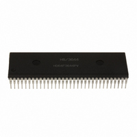
HD64F3644PV Renesas Electronics America, HD64F3644PV Datasheet - Page 185

HD64F3644PV
Manufacturer Part Number
HD64F3644PV
Description
IC H8/3644 MCU FLASH 32K 64SDIP
Manufacturer
Renesas Electronics America
Series
H8® H8/300Lr
Datasheet
1.HD64F3644HV.pdf
(551 pages)
Specifications of HD64F3644PV
Core Processor
H8/300L
Core Size
8-Bit
Speed
8MHz
Connectivity
SCI
Peripherals
PWM, WDT
Number Of I /o
53
Program Memory Size
32KB (32K x 8)
Program Memory Type
FLASH
Ram Size
1K x 8
Voltage - Supply (vcc/vdd)
2.7 V ~ 5.5 V
Data Converters
A/D 8x8b
Oscillator Type
Internal
Operating Temperature
-20°C ~ 75°C
Package / Case
64-SDIP (0.750", 19.05mm)
Lead Free Status / RoHS Status
Lead free / RoHS Compliant
Eeprom Size
-
Available stocks
Company
Part Number
Manufacturer
Quantity
Price
Company:
Part Number:
HD64F3644PV
Manufacturer:
Renesas Electronics America
Quantity:
135
- Current page: 185 of 551
- Download datasheet (4Mb)
7. Design a current margin into the programming voltage (V
8. Insure that peak overshoot at the FV
9. Use the recommended algorithms when programming and erasing flash memory.
10. For comments on interrupt handling while flash memory is being programmed or erased, see
11. Notes on accessing flash memory control registers
12 V
Insure that V
programming and erasing. Programming and erasing may become impossible outside this
range.
Connect bypass capacitors as close as possible to the FV
In boot mode start-up, also, bypass capacitors should be connected to the TEST pin in the same
way.
The recommended algorithms enable programming and erasing to be carried out without
subjecting the device to voltage stress or sacrificing program data reliability. When setting the
program (P) or erase (E) bit in the flash memory control register (FLMCR), the watchdog
timer should be set beforehand to prevent the specified time from being exceeded.
section 6.7.9, Interrupt Handling during Flash Memory Programming/Erasing.
a. Flash memory control register access state in each operating mode
b. To check for 12 V application/non-application in user mode
The H8/3644F, H8/3643F, and H8/3642AF have flash memory control registers located at
addresses H'FF80 (FLMCR), H'FF82 (EBR1), and H'FF83 (EBR2). These registers can
only be accessed when 12 V is applied to the flash memory programming power supply
pin, FV
When address H'FF80 is accessed in user mode, if 12 V is being applied to FV
is read/written to, and its initial value after reset is H'80. When 12 V is not being applied to
FV
7 (corresponding to the V
applied to FV
PP
1.0 F
, FLMCR is a reserved area that cannot be modified and always reads H'FF. Since bit
PP
PP
.
Figure 6.24 Example of V
remains within the range 12.0 V ±0.6 V (11.4 V to 12.6 V) during
PP
, application or release of 12 V to FV
PP
bit) is set to 1 at this time regardless of whether or not 12 V is
PP
0.01 F
and TEST pins does not exceed the maximum rating.
PP
Power Supply Circuit Design
Rev. 6.00 Sep 12, 2006 page 163 of 526
PP
PP
PP
and TEST pins.
cannot be determined simply from
) power supply.
FV
PP
REJ09B0326-0600
H8/3644F
Section 6 ROM
PP
, FLMCR
Related parts for HD64F3644PV
Image
Part Number
Description
Manufacturer
Datasheet
Request
R

Part Number:
Description:
(HD64 Series) Hitachi Single-Chip Microcomputer
Manufacturer:
Hitachi Semiconductor
Datasheet:

Part Number:
Description:
KIT STARTER FOR M16C/29
Manufacturer:
Renesas Electronics America
Datasheet:

Part Number:
Description:
KIT STARTER FOR R8C/2D
Manufacturer:
Renesas Electronics America
Datasheet:

Part Number:
Description:
R0K33062P STARTER KIT
Manufacturer:
Renesas Electronics America
Datasheet:

Part Number:
Description:
KIT STARTER FOR R8C/23 E8A
Manufacturer:
Renesas Electronics America
Datasheet:

Part Number:
Description:
KIT STARTER FOR R8C/25
Manufacturer:
Renesas Electronics America
Datasheet:

Part Number:
Description:
KIT STARTER H8S2456 SHARPE DSPLY
Manufacturer:
Renesas Electronics America
Datasheet:

Part Number:
Description:
KIT STARTER FOR R8C38C
Manufacturer:
Renesas Electronics America
Datasheet:

Part Number:
Description:
KIT STARTER FOR R8C35C
Manufacturer:
Renesas Electronics America
Datasheet:

Part Number:
Description:
KIT STARTER FOR R8CL3AC+LCD APPS
Manufacturer:
Renesas Electronics America
Datasheet:

Part Number:
Description:
KIT STARTER FOR RX610
Manufacturer:
Renesas Electronics America
Datasheet:

Part Number:
Description:
KIT STARTER FOR R32C/118
Manufacturer:
Renesas Electronics America
Datasheet:

Part Number:
Description:
KIT DEV RSK-R8C/26-29
Manufacturer:
Renesas Electronics America
Datasheet:

Part Number:
Description:
KIT STARTER FOR SH7124
Manufacturer:
Renesas Electronics America
Datasheet:

Part Number:
Description:
KIT STARTER FOR H8SX/1622
Manufacturer:
Renesas Electronics America
Datasheet:


