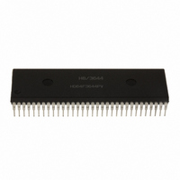
HD64F3644PV Renesas Electronics America, HD64F3644PV Datasheet - Page 278

HD64F3644PV
Manufacturer Part Number
HD64F3644PV
Description
IC H8/3644 MCU FLASH 32K 64SDIP
Manufacturer
Renesas Electronics America
Series
H8® H8/300Lr
Datasheet
1.HD64F3644HV.pdf
(551 pages)
Specifications of HD64F3644PV
Core Processor
H8/300L
Core Size
8-Bit
Speed
8MHz
Connectivity
SCI
Peripherals
PWM, WDT
Number Of I /o
53
Program Memory Size
32KB (32K x 8)
Program Memory Type
FLASH
Ram Size
1K x 8
Voltage - Supply (vcc/vdd)
2.7 V ~ 5.5 V
Data Converters
A/D 8x8b
Oscillator Type
Internal
Operating Temperature
-20°C ~ 75°C
Package / Case
64-SDIP (0.750", 19.05mm)
Lead Free Status / RoHS Status
Lead free / RoHS Compliant
Eeprom Size
-
Available stocks
Company
Part Number
Manufacturer
Quantity
Price
Company:
Part Number:
HD64F3644PV
Manufacturer:
Renesas Electronics America
Quantity:
135
- Current page: 278 of 551
- Download datasheet (4Mb)
Section 9 Timers
9.5.4
Timer X Operation
Rev. 6.00 Sep 12, 2006 page 256 of 526
REJ09B0326-0600
Output compare operation
Following a reset, FRC is initialized to H'0000 and starts counting up. Bits CKS1 and CKS0 in
TCRX can select one of three internal clock sources or an external clock for input to FRC. The
FRC contents are compared constantly with OCRA and OCRB. When a match occurs, the
output at pin FTOA or FTOB goes to the level selected by OLVLA or OLVLB in TOCR.
Following a reset, the output at both FTOA and FTOB is 0 until the first compare match. If
CCLRA is set to 1 in TCSRX, compare match A clears FRC to H'0000.
Input capture operation
Following a reset, FRC is initialized to H'0000 and starts counting up. Bits CKS1 and CKS0 in
TCRX can select one of three internal clock sources or an external clock for input to FRC.
When the edges selected by bits IEDGA to IEDGD in TCRX are input at pins FTIA to FTID,
the FRC value is transferred to ICRA to ICRD, and ICFA to ICFD are set to 1 in TCSRX. If
bits ICIAE to ICIDE are set to 1 in TIER, a CPU interrupt is requested.
If bits BUFEA and BUFEB are set to 1 in TCRX, ICRC and ICRD operate as buffer registers
for ICRA or ICRB. When the edges selected by bits IEDGA to IEDGD in TCRX are input at
pins FTIA and FTIB, the FRC value is transferred to ICRA or ICRB, and the previous value in
ICRA or ICRB is transferred to ICRC or ICRD. Simultaneously, ICFA or ICFB is set to 1. If
bit ICIAE or ICIBE is set to 1 in TIER, a CPU interrupt is requested.
Timer Operation
Related parts for HD64F3644PV
Image
Part Number
Description
Manufacturer
Datasheet
Request
R

Part Number:
Description:
(HD64 Series) Hitachi Single-Chip Microcomputer
Manufacturer:
Hitachi Semiconductor
Datasheet:

Part Number:
Description:
KIT STARTER FOR M16C/29
Manufacturer:
Renesas Electronics America
Datasheet:

Part Number:
Description:
KIT STARTER FOR R8C/2D
Manufacturer:
Renesas Electronics America
Datasheet:

Part Number:
Description:
R0K33062P STARTER KIT
Manufacturer:
Renesas Electronics America
Datasheet:

Part Number:
Description:
KIT STARTER FOR R8C/23 E8A
Manufacturer:
Renesas Electronics America
Datasheet:

Part Number:
Description:
KIT STARTER FOR R8C/25
Manufacturer:
Renesas Electronics America
Datasheet:

Part Number:
Description:
KIT STARTER H8S2456 SHARPE DSPLY
Manufacturer:
Renesas Electronics America
Datasheet:

Part Number:
Description:
KIT STARTER FOR R8C38C
Manufacturer:
Renesas Electronics America
Datasheet:

Part Number:
Description:
KIT STARTER FOR R8C35C
Manufacturer:
Renesas Electronics America
Datasheet:

Part Number:
Description:
KIT STARTER FOR R8CL3AC+LCD APPS
Manufacturer:
Renesas Electronics America
Datasheet:

Part Number:
Description:
KIT STARTER FOR RX610
Manufacturer:
Renesas Electronics America
Datasheet:

Part Number:
Description:
KIT STARTER FOR R32C/118
Manufacturer:
Renesas Electronics America
Datasheet:

Part Number:
Description:
KIT DEV RSK-R8C/26-29
Manufacturer:
Renesas Electronics America
Datasheet:

Part Number:
Description:
KIT STARTER FOR SH7124
Manufacturer:
Renesas Electronics America
Datasheet:

Part Number:
Description:
KIT STARTER FOR H8SX/1622
Manufacturer:
Renesas Electronics America
Datasheet:


