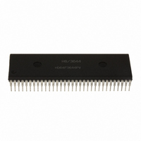
HD64F3644PV Renesas Electronics America, HD64F3644PV Datasheet - Page 374

HD64F3644PV
Manufacturer Part Number
HD64F3644PV
Description
IC H8/3644 MCU FLASH 32K 64SDIP
Manufacturer
Renesas Electronics America
Series
H8® H8/300Lr
Datasheet
1.HD64F3644HV.pdf
(551 pages)
Specifications of HD64F3644PV
Core Processor
H8/300L
Core Size
8-Bit
Speed
8MHz
Connectivity
SCI
Peripherals
PWM, WDT
Number Of I /o
53
Program Memory Size
32KB (32K x 8)
Program Memory Type
FLASH
Ram Size
1K x 8
Voltage - Supply (vcc/vdd)
2.7 V ~ 5.5 V
Data Converters
A/D 8x8b
Oscillator Type
Internal
Operating Temperature
-20°C ~ 75°C
Package / Case
64-SDIP (0.750", 19.05mm)
Lead Free Status / RoHS Status
Lead free / RoHS Compliant
Eeprom Size
-
Available stocks
Company
Part Number
Manufacturer
Quantity
Price
Company:
Part Number:
HD64F3644PV
Manufacturer:
Renesas Electronics America
Quantity:
135
- Current page: 374 of 551
- Download datasheet (4Mb)
Section 12 A/D Converter
12.4
When A/D conversion ends (ADSF changes from 1 to 0), bit IRRAD in interrupt request
register 2 (IRR2) is set to 1.
A/D conversion end interrupts can be enabled or disabled by means of bit IENAD in interrupt
enable register 2 (IENR2).
For further details see section 3.3, Interrupts.
12.5
An example of how the A/D converter can be used is given below, using channel 1 (pin AN1) as
the analog input channel. Figure 12.3 shows the operation timing.
1. Bits CH3 to CH0 of the A/D mode register (AMR) are set to 0101, making pin AN1 the analog
2. When A/D conversion is complete, bit IRRAD is set to 1, and the A/D conversion result is
3. Bit IENAD = 1, so an A/D conversion end interrupt is requested.
4. The A/D interrupt handling routine starts.
5. The A/D conversion result is read and processed.
6. The A/D interrupt handling routine ends.
If ADSF is set to 1 again afterward, A/D conversion starts and steps 2 through 6 take place.
Figures 12.4 and 12.5 show flow charts of procedures for using the A/D converter.
Rev. 6.00 Sep 12, 2006 page 352 of 526
REJ09B0326-0600
input channel. A/D interrupts are enabled by setting bit IENAD to 1, and A/D conversion is
started by setting bit ADSF to 1.
stored in the A/D result register (ADRR). At the same time ADSF is cleared to 0, and the A/D
converter goes to the idle state.
Pin ADTRG
(when bit
INTEG5 = 0)
ADSF
Interrupts
Typical Use
Figure 12.2 External Trigger Input Timing
A/D conversion
Related parts for HD64F3644PV
Image
Part Number
Description
Manufacturer
Datasheet
Request
R

Part Number:
Description:
(HD64 Series) Hitachi Single-Chip Microcomputer
Manufacturer:
Hitachi Semiconductor
Datasheet:

Part Number:
Description:
KIT STARTER FOR M16C/29
Manufacturer:
Renesas Electronics America
Datasheet:

Part Number:
Description:
KIT STARTER FOR R8C/2D
Manufacturer:
Renesas Electronics America
Datasheet:

Part Number:
Description:
R0K33062P STARTER KIT
Manufacturer:
Renesas Electronics America
Datasheet:

Part Number:
Description:
KIT STARTER FOR R8C/23 E8A
Manufacturer:
Renesas Electronics America
Datasheet:

Part Number:
Description:
KIT STARTER FOR R8C/25
Manufacturer:
Renesas Electronics America
Datasheet:

Part Number:
Description:
KIT STARTER H8S2456 SHARPE DSPLY
Manufacturer:
Renesas Electronics America
Datasheet:

Part Number:
Description:
KIT STARTER FOR R8C38C
Manufacturer:
Renesas Electronics America
Datasheet:

Part Number:
Description:
KIT STARTER FOR R8C35C
Manufacturer:
Renesas Electronics America
Datasheet:

Part Number:
Description:
KIT STARTER FOR R8CL3AC+LCD APPS
Manufacturer:
Renesas Electronics America
Datasheet:

Part Number:
Description:
KIT STARTER FOR RX610
Manufacturer:
Renesas Electronics America
Datasheet:

Part Number:
Description:
KIT STARTER FOR R32C/118
Manufacturer:
Renesas Electronics America
Datasheet:

Part Number:
Description:
KIT DEV RSK-R8C/26-29
Manufacturer:
Renesas Electronics America
Datasheet:

Part Number:
Description:
KIT STARTER FOR SH7124
Manufacturer:
Renesas Electronics America
Datasheet:

Part Number:
Description:
KIT STARTER FOR H8SX/1622
Manufacturer:
Renesas Electronics America
Datasheet:


