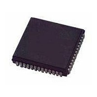
MC68HC711E9MFNE2 Freescale Semiconductor, MC68HC711E9MFNE2 Datasheet - Page 61

MC68HC711E9MFNE2
Manufacturer Part Number
MC68HC711E9MFNE2
Description
IC MCU 8BIT 512BYTES ROM 52-PLCC
Manufacturer
Freescale Semiconductor
Series
HC11r
Specifications of MC68HC711E9MFNE2
Core Processor
HC11
Core Size
8-Bit
Speed
2MHz
Connectivity
SCI, SPI
Peripherals
POR, WDT
Number Of I /o
38
Program Memory Size
12KB (12K x 8)
Program Memory Type
OTP
Eeprom Size
512 x 8
Ram Size
512 x 8
Voltage - Supply (vcc/vdd)
4.5 V ~ 5.5 V
Data Converters
A/D 8x8b
Oscillator Type
Internal
Operating Temperature
-40°C ~ 125°C
Package / Case
52-PLCC
Processor Series
HC711E
Core
HC11
Data Bus Width
8 bit
Data Ram Size
512 B
Interface Type
SCI, SPI
Maximum Clock Frequency
2 MHz
Number Of Programmable I/os
38
Number Of Timers
8
Maximum Operating Temperature
+ 125 C
Mounting Style
SMD/SMT
Minimum Operating Temperature
- 40 C
On-chip Adc
8 bit
Lead Free Status / RoHS Status
Lead free / RoHS Compliant
Available stocks
Company
Part Number
Manufacturer
Quantity
Price
Company:
Part Number:
MC68HC711E9MFNE2
Manufacturer:
TI
Quantity:
167
Company:
Part Number:
MC68HC711E9MFNE2
Manufacturer:
Freescale Semiconductor
Quantity:
10 000
- Current page: 61 of 242
- Download datasheet (2Mb)
3.4 Conversion Process
The A/D conversion sequence begins one E-clock cycle after a write to the A/D control/status register,
ADCTL. The bits in ADCTL select the channel and the mode of conversion.
An input voltage equal to V
scale), with no overflow indication. For ratiometric conversions of this type, the source of each analog
input should use V
3.5 Channel Assignments
The multiplexer allows the A/D converter to select one of 16 analog signals. Eight of these channels
correspond to port E input lines to the MCU, four of the channels are internal reference points or test
functions, and four channels are reserved. Refer to
3.6 Single-Channel Operation
The two types of single-channel operation are:
Freescale Semiconductor
1. When SCAN = 0, the single selected channel is converted four consecutive times. The first result
2. When SCAN = 1, conversions continue to be performed on the selected channel with the fifth
is stored in A/D result register 1 (ADR1), and the fourth result is stored in ADR4. After the fourth
conversion is complete, all conversion activity is halted until a new conversion command is written
to the ADCTL register.
conversion being stored in register ADR1 (overwriting the first conversion result), the sixth
conversion overwriting ADR2, and so on.
RH
as the supply voltage and be referenced to V
1. Used for factory testing
RL
Table 3-1. Converter Channel Assignments
Channel
Number
converts to $00 and an input voltage equal to V
9 – 12
13
14
15
16
1
2
3
4
5
6
7
8
M68HC11E Family Data Sheet, Rev. 5.1
Reserved
Reserved
(V
Channel
Signal
V
V
RH
AN0
AN1
AN2
AN3
AN4
AN5
AN6
AN7
RH
RL
Table
)/2
(1)
(1)
(1)
(1)
3-1.
Result in ADRx
if MULT = 1
RL
ADR1
ADR2
ADR3
ADR4
ADR1
ADR2
ADR3
ADR4
ADR1
ADR2
ADR3
ADR4
.
—
RH
converts to $FF (full
Conversion Process
61
Related parts for MC68HC711E9MFNE2
Image
Part Number
Description
Manufacturer
Datasheet
Request
R

Part Number:
Description:
APPENDIX A ELECTRICAL CHARACTERISTICS
Manufacturer:
FREESCALE [Freescale Semiconductor, Inc]
Datasheet:
Part Number:
Description:
Manufacturer:
Freescale Semiconductor, Inc
Datasheet:
Part Number:
Description:
Manufacturer:
Freescale Semiconductor, Inc
Datasheet:
Part Number:
Description:
Manufacturer:
Freescale Semiconductor, Inc
Datasheet:
Part Number:
Description:
Manufacturer:
Freescale Semiconductor, Inc
Datasheet:
Part Number:
Description:
Manufacturer:
Freescale Semiconductor, Inc
Datasheet:
Part Number:
Description:
Manufacturer:
Freescale Semiconductor, Inc
Datasheet:
Part Number:
Description:
Manufacturer:
Freescale Semiconductor, Inc
Datasheet:
Part Number:
Description:
Manufacturer:
Freescale Semiconductor, Inc
Datasheet:
Part Number:
Description:
Manufacturer:
Freescale Semiconductor, Inc
Datasheet:
Part Number:
Description:
Manufacturer:
Freescale Semiconductor, Inc
Datasheet:
Part Number:
Description:
Manufacturer:
Freescale Semiconductor, Inc
Datasheet:
Part Number:
Description:
Manufacturer:
Freescale Semiconductor, Inc
Datasheet:
Part Number:
Description:
Manufacturer:
Freescale Semiconductor, Inc
Datasheet:
Part Number:
Description:
Manufacturer:
Freescale Semiconductor, Inc
Datasheet:


