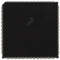
MC68HC711E9CFNE2 Freescale Semiconductor, MC68HC711E9CFNE2 Datasheet - Page 213

MC68HC711E9CFNE2
Manufacturer Part Number
MC68HC711E9CFNE2
Description
IC MCU 8BIT 512RAM 52-PLC
Manufacturer
Freescale Semiconductor
Series
HC11r
Datasheet
1.MC68HC711E9CFNE3.pdf
(336 pages)
Specifications of MC68HC711E9CFNE2
Core Processor
HC11
Core Size
8-Bit
Speed
2MHz
Connectivity
SCI, SPI
Peripherals
POR, WDT
Number Of I /o
38
Program Memory Size
12KB (12K x 8)
Program Memory Type
OTP
Eeprom Size
512 x 8
Ram Size
512 x 8
Voltage - Supply (vcc/vdd)
4.5 V ~ 5.5 V
Data Converters
A/D 8x8b
Oscillator Type
Internal
Operating Temperature
-40°C ~ 85°C
Package / Case
52-PLCC
Processor Series
HC711E
Core
HC11
Data Bus Width
8 bit
Data Ram Size
512 B
Interface Type
SCI, SPI
Maximum Clock Frequency
2 MHz
Number Of Programmable I/os
38
Number Of Timers
8
Maximum Operating Temperature
+ 85 C
Mounting Style
SMD/SMT
Minimum Operating Temperature
- 40 C
On-chip Adc
8 bit
Lead Free Status / RoHS Status
Lead free / RoHS Compliant
Available stocks
Company
Part Number
Manufacturer
Quantity
Price
Company:
Part Number:
MC68HC711E9CFNE2
Manufacturer:
TE
Quantity:
12 000
Company:
Part Number:
MC68HC711E9CFNE2
Manufacturer:
FREESCAL
Quantity:
5 530
- Current page: 213 of 336
- Download datasheet (4Mb)
10.3.5 A/D Converter Clocks
10.3.6 Conversion Sequence
M68HC11E Family — Rev. 3.2
MOTOROLA
E CLOCK
0
CHANNEL, UPDATE
CONVERT FIRST
SAMPLE ANALOG INPUT
ADR1
12 E CYCLES
The CSEL bit in the OPTION register selects whether the A/D converter
uses the system E clock or an internal RC oscillator for synchronization.
When E-clock frequency is below 750 kHz, charge leakage in the
capacitor array can cause errors, and the internal oscillator should be
used. When the RC clock is used, additional errors can occur because
the comparator is sensitive to the additional system clock noise.
A/D converter operations are performed in sequences of four
conversions each. A conversion sequence can repeat continuously or
stop after one iteration. The conversion complete flag (CCF) is set after
the fourth conversion in a sequence to show the availability of data in the
result registers.
Synchronization is referenced to the system E clock.
Figure 10-3. A/D Conversion Sequence
32
CONVERT SECOND
CHANNEL, UPDATE
Analog-to-Digital (A/D) Converter
ADR2
CYCLES
MSB
4
Figure 10-3
SUCCESSIVE APPROXIMATION SEQUENCE
BIT 6
CYC
64
2
BIT 5
CYC
CHANNEL, UPDATE
CONVERT THIRD
2
shows the timing of a typical sequence.
BIT 4
CYC
ADR3
2
BIT 3
CYC
2
BIT 2
CYC
2
96
BIT 1
CYC
CHANNEL, UPDATE
CONVERT FOURTH
2
Analog-to-Digital (A/D) Converter
CYC
LSB
ADR4
2
CYC
END
2
128 — E CYCLES
Technical Data
Overview
213
Related parts for MC68HC711E9CFNE2
Image
Part Number
Description
Manufacturer
Datasheet
Request
R

Part Number:
Description:
APPENDIX A ELECTRICAL CHARACTERISTICS
Manufacturer:
FREESCALE [Freescale Semiconductor, Inc]
Datasheet:
Part Number:
Description:
Manufacturer:
Freescale Semiconductor, Inc
Datasheet:
Part Number:
Description:
Manufacturer:
Freescale Semiconductor, Inc
Datasheet:
Part Number:
Description:
Manufacturer:
Freescale Semiconductor, Inc
Datasheet:
Part Number:
Description:
Manufacturer:
Freescale Semiconductor, Inc
Datasheet:
Part Number:
Description:
Manufacturer:
Freescale Semiconductor, Inc
Datasheet:
Part Number:
Description:
Manufacturer:
Freescale Semiconductor, Inc
Datasheet:
Part Number:
Description:
Manufacturer:
Freescale Semiconductor, Inc
Datasheet:
Part Number:
Description:
Manufacturer:
Freescale Semiconductor, Inc
Datasheet:
Part Number:
Description:
Manufacturer:
Freescale Semiconductor, Inc
Datasheet:
Part Number:
Description:
Manufacturer:
Freescale Semiconductor, Inc
Datasheet:
Part Number:
Description:
Manufacturer:
Freescale Semiconductor, Inc
Datasheet:
Part Number:
Description:
Manufacturer:
Freescale Semiconductor, Inc
Datasheet:
Part Number:
Description:
Manufacturer:
Freescale Semiconductor, Inc
Datasheet:
Part Number:
Description:
Manufacturer:
Freescale Semiconductor, Inc
Datasheet:


