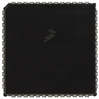
MC68HC711E9CFNE2 Freescale Semiconductor, MC68HC711E9CFNE2 Datasheet - Page 294

MC68HC711E9CFNE2
Manufacturer Part Number
MC68HC711E9CFNE2
Description
IC MCU 8BIT 512RAM 52-PLC
Manufacturer
Freescale Semiconductor
Series
HC11r
Datasheet
1.MC68HC711E9CFNE3.pdf
(336 pages)
Specifications of MC68HC711E9CFNE2
Core Processor
HC11
Core Size
8-Bit
Speed
2MHz
Connectivity
SCI, SPI
Peripherals
POR, WDT
Number Of I /o
38
Program Memory Size
12KB (12K x 8)
Program Memory Type
OTP
Eeprom Size
512 x 8
Ram Size
512 x 8
Voltage - Supply (vcc/vdd)
4.5 V ~ 5.5 V
Data Converters
A/D 8x8b
Oscillator Type
Internal
Operating Temperature
-40°C ~ 85°C
Package / Case
52-PLCC
Processor Series
HC711E
Core
HC11
Data Bus Width
8 bit
Data Ram Size
512 B
Interface Type
SCI, SPI
Maximum Clock Frequency
2 MHz
Number Of Programmable I/os
38
Number Of Timers
8
Maximum Operating Temperature
+ 85 C
Mounting Style
SMD/SMT
Minimum Operating Temperature
- 40 C
On-chip Adc
8 bit
Lead Free Status / RoHS Status
Lead free / RoHS Compliant
Available stocks
Company
Part Number
Manufacturer
Quantity
Price
Company:
Part Number:
MC68HC711E9CFNE2
Manufacturer:
TE
Quantity:
12 000
Company:
Part Number:
MC68HC711E9CFNE2
Manufacturer:
FREESCAL
Quantity:
5 530
- Current page: 294 of 336
- Download datasheet (4Mb)
Application Note
Other
Driving Boot Mode from Another M68HC11
294
series resistor will prevent direct conflict between the internal TxD driver
and the external driver connected to PD1 through the series resistor.
The bootloader firmware sets the DWOM control bit, which configures all
port D pins for wire-OR operation. During the bootloading process, all
port D pins except the PD1/TxD pin are configured as high-impedance
inputs. Any port D pin that normally is used as an output should have a
pullup resistor so it does not float during the bootloading process.
A second M68HC11 system can easily act as the host to drive bootstrap
loading of an M68HC11 MCU. This method is used to examine and
program non-volatile memories in target M68HC11s in Motorola EVMs.
The following hardware and software example will demonstrate this and
other bootstrap mode features.
The schematic in
duplicator for the MC68HC711E9. The circuitry is built in the wire-wrap
area of an M68HC11EVBU evaluation board to simplify construction.
The schematic shows only the important portions of the EVBU circuitry
to avoid confusion. To see the complete EVBU schematic, refer to the
M68HC11EVBU Universal Evaluation Board User’s Manual, Motorola
document order number M68HC11EVBU/D.
The default configuration of the EVBU must be changed to make the
appropriate connections to the circuitry in the wire-wrap area and to
configure the master MCU for bootstrap mode. A fabricated jumper must
be installed at J6 to connect the XTAL output of the master MCU to the
wire-wrap connector P5, which has been wired to the EXTAL input of the
target MCU. Cut traces that short across J8 and J9 must be cut on the
solder side of the printed circuit board to disconnect the normal SCI
connections to the RS232 level translator (U4) of the EVBU. The J8 and
J9 connections can be restored easily at a later time by installing
fabricated jumpers on the component side of the board. A fabricated
Figure 6
shows the circuitry for a simple EPROM
AN1060 — Rev. 1.0
MOTOROLA
Related parts for MC68HC711E9CFNE2
Image
Part Number
Description
Manufacturer
Datasheet
Request
R

Part Number:
Description:
APPENDIX A ELECTRICAL CHARACTERISTICS
Manufacturer:
FREESCALE [Freescale Semiconductor, Inc]
Datasheet:
Part Number:
Description:
Manufacturer:
Freescale Semiconductor, Inc
Datasheet:
Part Number:
Description:
Manufacturer:
Freescale Semiconductor, Inc
Datasheet:
Part Number:
Description:
Manufacturer:
Freescale Semiconductor, Inc
Datasheet:
Part Number:
Description:
Manufacturer:
Freescale Semiconductor, Inc
Datasheet:
Part Number:
Description:
Manufacturer:
Freescale Semiconductor, Inc
Datasheet:
Part Number:
Description:
Manufacturer:
Freescale Semiconductor, Inc
Datasheet:
Part Number:
Description:
Manufacturer:
Freescale Semiconductor, Inc
Datasheet:
Part Number:
Description:
Manufacturer:
Freescale Semiconductor, Inc
Datasheet:
Part Number:
Description:
Manufacturer:
Freescale Semiconductor, Inc
Datasheet:
Part Number:
Description:
Manufacturer:
Freescale Semiconductor, Inc
Datasheet:
Part Number:
Description:
Manufacturer:
Freescale Semiconductor, Inc
Datasheet:
Part Number:
Description:
Manufacturer:
Freescale Semiconductor, Inc
Datasheet:
Part Number:
Description:
Manufacturer:
Freescale Semiconductor, Inc
Datasheet:
Part Number:
Description:
Manufacturer:
Freescale Semiconductor, Inc
Datasheet:


