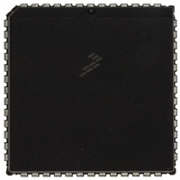
MC68HC711E9CFNE2 Freescale Semiconductor, MC68HC711E9CFNE2 Datasheet - Page 39

MC68HC711E9CFNE2
Manufacturer Part Number
MC68HC711E9CFNE2
Description
IC MCU 8BIT 512RAM 52-PLC
Manufacturer
Freescale Semiconductor
Series
HC11r
Datasheet
1.MC68HC711E9CFNE3.pdf
(336 pages)
Specifications of MC68HC711E9CFNE2
Core Processor
HC11
Core Size
8-Bit
Speed
2MHz
Connectivity
SCI, SPI
Peripherals
POR, WDT
Number Of I /o
38
Program Memory Size
12KB (12K x 8)
Program Memory Type
OTP
Eeprom Size
512 x 8
Ram Size
512 x 8
Voltage - Supply (vcc/vdd)
4.5 V ~ 5.5 V
Data Converters
A/D 8x8b
Oscillator Type
Internal
Operating Temperature
-40°C ~ 85°C
Package / Case
52-PLCC
Processor Series
HC711E
Core
HC11
Data Bus Width
8 bit
Data Ram Size
512 B
Interface Type
SCI, SPI
Maximum Clock Frequency
2 MHz
Number Of Programmable I/os
38
Number Of Timers
8
Maximum Operating Temperature
+ 85 C
Mounting Style
SMD/SMT
Minimum Operating Temperature
- 40 C
On-chip Adc
8 bit
Lead Free Status / RoHS Status
Lead free / RoHS Compliant
Available stocks
Company
Part Number
Manufacturer
Quantity
Price
Company:
Part Number:
MC68HC711E9CFNE2
Manufacturer:
TE
Quantity:
12 000
Company:
Part Number:
MC68HC711E9CFNE2
Manufacturer:
FREESCAL
Quantity:
5 530
- Current page: 39 of 336
- Download datasheet (4Mb)
2.13 Port Signals
2.13.1 Port A
M68HC11E Family — Rev. 3.2
MOTOROLA
indicates that a read cycle is in progress. R/W stays low during
consecutive data bus write cycles, such as a double-byte store. It is
possible for data to be driven out of port C, if internal read visibility (IRV)
is enabled and an internal address is read, even though R/W is in a
high-impedance state. Refer to
On-Chip Memory
visibility not E).
Port pins have different functions in different operating modes. Pin
functions for port A, port D, and port E are independent of operating
modes. Port B and port C, however, are affected by operating mode.
Port B provides eight general-purpose output signals in single-chip
operating modes. When the microcontroller is in expanded multiplexed
operating mode, port B pins are the eight high-order address lines.
Port C provides eight general-purpose input/output signals when the
MCU is in the single-chip operating mode. When the microcontroller is in
the expanded multiplexed operating mode, port C pins are a multiplexed
address/data bus.
Refer to
within different operating modes. Terminate unused inputs and
input/output (I/O) pins configured as inputs high or low.
In all operating modes, port A can be configured for three timer input
capture (IC) functions and four timer output compare (OC) functions. An
additional pin can be configured as either the fourth IC or the fifth OC.
Any port A pin that is not currently being used for a timer function can be
used as either a general-purpose input or output line. Only port A pins
PA7 and PA3 have an associated data direction control bit that allows
the pin to be selectively configured as input or output. Bits DDRA7 and
DDRA3 located in PACTL register control data direction for PA7 and
PA3, respectively. All other port A pins are fixed as either input or output.
Table 2-1
Pin Descriptions
for more information about IRVNE (internal read
for a functional description of the 40 port signals
Section 4. Operating Modes and
Pin Descriptions
Technical Data
Port Signals
39
Related parts for MC68HC711E9CFNE2
Image
Part Number
Description
Manufacturer
Datasheet
Request
R

Part Number:
Description:
APPENDIX A ELECTRICAL CHARACTERISTICS
Manufacturer:
FREESCALE [Freescale Semiconductor, Inc]
Datasheet:
Part Number:
Description:
Manufacturer:
Freescale Semiconductor, Inc
Datasheet:
Part Number:
Description:
Manufacturer:
Freescale Semiconductor, Inc
Datasheet:
Part Number:
Description:
Manufacturer:
Freescale Semiconductor, Inc
Datasheet:
Part Number:
Description:
Manufacturer:
Freescale Semiconductor, Inc
Datasheet:
Part Number:
Description:
Manufacturer:
Freescale Semiconductor, Inc
Datasheet:
Part Number:
Description:
Manufacturer:
Freescale Semiconductor, Inc
Datasheet:
Part Number:
Description:
Manufacturer:
Freescale Semiconductor, Inc
Datasheet:
Part Number:
Description:
Manufacturer:
Freescale Semiconductor, Inc
Datasheet:
Part Number:
Description:
Manufacturer:
Freescale Semiconductor, Inc
Datasheet:
Part Number:
Description:
Manufacturer:
Freescale Semiconductor, Inc
Datasheet:
Part Number:
Description:
Manufacturer:
Freescale Semiconductor, Inc
Datasheet:
Part Number:
Description:
Manufacturer:
Freescale Semiconductor, Inc
Datasheet:
Part Number:
Description:
Manufacturer:
Freescale Semiconductor, Inc
Datasheet:
Part Number:
Description:
Manufacturer:
Freescale Semiconductor, Inc
Datasheet:


