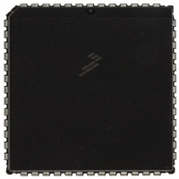
MC68HC711E9CFNE2 Freescale Semiconductor, MC68HC711E9CFNE2 Datasheet - Page 41

MC68HC711E9CFNE2
Manufacturer Part Number
MC68HC711E9CFNE2
Description
IC MCU 8BIT 512RAM 52-PLC
Manufacturer
Freescale Semiconductor
Series
HC11r
Datasheet
1.MC68HC711E9CFNE3.pdf
(336 pages)
Specifications of MC68HC711E9CFNE2
Core Processor
HC11
Core Size
8-Bit
Speed
2MHz
Connectivity
SCI, SPI
Peripherals
POR, WDT
Number Of I /o
38
Program Memory Size
12KB (12K x 8)
Program Memory Type
OTP
Eeprom Size
512 x 8
Ram Size
512 x 8
Voltage - Supply (vcc/vdd)
4.5 V ~ 5.5 V
Data Converters
A/D 8x8b
Oscillator Type
Internal
Operating Temperature
-40°C ~ 85°C
Package / Case
52-PLCC
Processor Series
HC711E
Core
HC11
Data Bus Width
8 bit
Data Ram Size
512 B
Interface Type
SCI, SPI
Maximum Clock Frequency
2 MHz
Number Of Programmable I/os
38
Number Of Timers
8
Maximum Operating Temperature
+ 85 C
Mounting Style
SMD/SMT
Minimum Operating Temperature
- 40 C
On-chip Adc
8 bit
Lead Free Status / RoHS Status
Lead free / RoHS Compliant
Available stocks
Company
Part Number
Manufacturer
Quantity
Price
Company:
Part Number:
MC68HC711E9CFNE2
Manufacturer:
TE
Quantity:
12 000
Company:
Part Number:
MC68HC711E9CFNE2
Manufacturer:
FREESCAL
Quantity:
5 530
- Current page: 41 of 336
- Download datasheet (4Mb)
2.13.2 Port B
M68HC11E Family — Rev. 3.2
MOTOROLA
PA7 can function as general-purpose I/O or as timer output compare for
OC1. PA7 is also the input to the pulse accumulator, even while
functioning as a general-purpose I/O or an OC1 output.
PA6–PA4 serve as either general-purpose outputs, timer input captures,
or timer output compare 2–4. In addition, PA6–PA4 can be controlled by
OC1.
PA3 can be a general-purpose I/O pin or a timer IC/OC pin. Timer
functions associated with this pin include OC1 and IC4/OC5. IC4/OC5 is
software selectable as either a fourth input capture or a fifth output
compare. PA3 can also be configured to allow OC1 edges to trigger IC4
captures.
PA2–PA0 serve as general-purpose inputs or as IC1–IC3.
PORTA can be read at any time. Reads of pins configured as inputs
return the logic level present on the pin. Pins configured as outputs
return the logic level present at the pin driver input. If written, PORTA
stores the data in an internal latch, bits 7 and 3. It drives the pins only if
they are configured as outputs. Writes to PORTA do not change the pin
state when pins are configured for timer input captures or output
compares. Refer to
During single-chip operating modes, all port B pins are general-purpose
output pins. During MCU reads of this port, the level sensed at the input
side of the port B output drivers is read. Port B can also be used in simple
strobed output mode. In this mode, an output pulse appears at the STRB
signal each time data is written to port B.
In expanded multiplexed operating modes, all of the port B pins act as
high order address output signals. During each MCU cycle, bits 15–8 of
the address bus are output on the PB7–PB0 pins. The PORTB register
is treated as an external address in expanded modes.
Pin Descriptions
Section 6. Parallel Input/Output (I/O)
Pin Descriptions
Technical Data
Ports.
Port Signals
41
Related parts for MC68HC711E9CFNE2
Image
Part Number
Description
Manufacturer
Datasheet
Request
R

Part Number:
Description:
APPENDIX A ELECTRICAL CHARACTERISTICS
Manufacturer:
FREESCALE [Freescale Semiconductor, Inc]
Datasheet:
Part Number:
Description:
Manufacturer:
Freescale Semiconductor, Inc
Datasheet:
Part Number:
Description:
Manufacturer:
Freescale Semiconductor, Inc
Datasheet:
Part Number:
Description:
Manufacturer:
Freescale Semiconductor, Inc
Datasheet:
Part Number:
Description:
Manufacturer:
Freescale Semiconductor, Inc
Datasheet:
Part Number:
Description:
Manufacturer:
Freescale Semiconductor, Inc
Datasheet:
Part Number:
Description:
Manufacturer:
Freescale Semiconductor, Inc
Datasheet:
Part Number:
Description:
Manufacturer:
Freescale Semiconductor, Inc
Datasheet:
Part Number:
Description:
Manufacturer:
Freescale Semiconductor, Inc
Datasheet:
Part Number:
Description:
Manufacturer:
Freescale Semiconductor, Inc
Datasheet:
Part Number:
Description:
Manufacturer:
Freescale Semiconductor, Inc
Datasheet:
Part Number:
Description:
Manufacturer:
Freescale Semiconductor, Inc
Datasheet:
Part Number:
Description:
Manufacturer:
Freescale Semiconductor, Inc
Datasheet:
Part Number:
Description:
Manufacturer:
Freescale Semiconductor, Inc
Datasheet:
Part Number:
Description:
Manufacturer:
Freescale Semiconductor, Inc
Datasheet:


