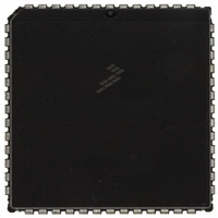
MC68HC711E9CFNE2 Freescale Semiconductor, MC68HC711E9CFNE2 Datasheet - Page 89

MC68HC711E9CFNE2
Manufacturer Part Number
MC68HC711E9CFNE2
Description
IC MCU 8BIT 512RAM 52-PLC
Manufacturer
Freescale Semiconductor
Series
HC11r
Datasheet
1.MC68HC711E9CFNE3.pdf
(336 pages)
Specifications of MC68HC711E9CFNE2
Core Processor
HC11
Core Size
8-Bit
Speed
2MHz
Connectivity
SCI, SPI
Peripherals
POR, WDT
Number Of I /o
38
Program Memory Size
12KB (12K x 8)
Program Memory Type
OTP
Eeprom Size
512 x 8
Ram Size
512 x 8
Voltage - Supply (vcc/vdd)
4.5 V ~ 5.5 V
Data Converters
A/D 8x8b
Oscillator Type
Internal
Operating Temperature
-40°C ~ 85°C
Package / Case
52-PLCC
Processor Series
HC711E
Core
HC11
Data Bus Width
8 bit
Data Ram Size
512 B
Interface Type
SCI, SPI
Maximum Clock Frequency
2 MHz
Number Of Programmable I/os
38
Number Of Timers
8
Maximum Operating Temperature
+ 85 C
Mounting Style
SMD/SMT
Minimum Operating Temperature
- 40 C
On-chip Adc
8 bit
Lead Free Status / RoHS Status
Lead free / RoHS Compliant
Available stocks
Company
Part Number
Manufacturer
Quantity
Price
Company:
Part Number:
MC68HC711E9CFNE2
Manufacturer:
TE
Quantity:
12 000
Company:
Part Number:
MC68HC711E9CFNE2
Manufacturer:
FREESCAL
Quantity:
5 530
- Current page: 89 of 336
- Download datasheet (4Mb)
4.4.3.2 RAM and I/O Mapping Register
M68HC11E Family — Rev. 3.2
MOTOROLA
ROMON — ROM/EPROM/OTPROM Enable Bit
EEON — EEPROM Enable Bit
The internal registers used to control the operation of the MCU can be
relocated on 4-Kbyte boundaries within the memory space with the use
of the RAM and I/O mapping register (INIT). This 8-bit special-purpose
register can change the default locations of the RAM and control
registers within the MCU memory map. It can be written only once within
the first 64 E-clock cycles after a reset in normal modes, and then it
becomes a read-only register.
RAM[3:0] — RAM Map Position Bits
Address:
Reset:
Read:
Write:
When this bit is 0, the ROM or EPROM is disabled and that memory
space becomes externally addressed. In single-chip mode, ROMON
is forced to 1 to enable ROM/EPROM regardless of the state of the
ROMON bit.
When this bit is 0, the EEPROM is disabled and that memory space
becomes externally addressed.
These four bits, which specify the upper hexadecimal digit of the RAM
address, control position of RAM in the memory map. RAM can be
positioned at the beginning of any 4-Kbyte page in the memory map.
It is initialized to address $0000 out of reset. Refer to
0 = ROM disabled from the memory map
1 = ROM present in the memory map
0 = EEPROM removed from the memory map
1 = EEPROM present in the memory map
Operating Modes and On-Chip Memory
Figure 4-12. RAM and I/O Mapping Register (INIT)
$103D
RAM3
Bit 7
0
RAM2
6
0
RAM1
5
0
RAM0
4
0
Operating Modes and On-Chip Memory
REG3
3
0
REG2
2
0
Table
REG1
Technical Data
1
0
Memory Map
4-4.
REG0
Bit 0
1
89
Related parts for MC68HC711E9CFNE2
Image
Part Number
Description
Manufacturer
Datasheet
Request
R

Part Number:
Description:
APPENDIX A ELECTRICAL CHARACTERISTICS
Manufacturer:
FREESCALE [Freescale Semiconductor, Inc]
Datasheet:
Part Number:
Description:
Manufacturer:
Freescale Semiconductor, Inc
Datasheet:
Part Number:
Description:
Manufacturer:
Freescale Semiconductor, Inc
Datasheet:
Part Number:
Description:
Manufacturer:
Freescale Semiconductor, Inc
Datasheet:
Part Number:
Description:
Manufacturer:
Freescale Semiconductor, Inc
Datasheet:
Part Number:
Description:
Manufacturer:
Freescale Semiconductor, Inc
Datasheet:
Part Number:
Description:
Manufacturer:
Freescale Semiconductor, Inc
Datasheet:
Part Number:
Description:
Manufacturer:
Freescale Semiconductor, Inc
Datasheet:
Part Number:
Description:
Manufacturer:
Freescale Semiconductor, Inc
Datasheet:
Part Number:
Description:
Manufacturer:
Freescale Semiconductor, Inc
Datasheet:
Part Number:
Description:
Manufacturer:
Freescale Semiconductor, Inc
Datasheet:
Part Number:
Description:
Manufacturer:
Freescale Semiconductor, Inc
Datasheet:
Part Number:
Description:
Manufacturer:
Freescale Semiconductor, Inc
Datasheet:
Part Number:
Description:
Manufacturer:
Freescale Semiconductor, Inc
Datasheet:
Part Number:
Description:
Manufacturer:
Freescale Semiconductor, Inc
Datasheet:


