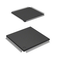
DF2161BVTE10 Renesas Electronics America, DF2161BVTE10 Datasheet - Page 469

DF2161BVTE10
Manufacturer Part Number
DF2161BVTE10
Description
MCU 3V 128K 144-TQFP
Manufacturer
Renesas Electronics America
Series
H8® H8S/2100r
Datasheet
1.DF2160BVT10V.pdf
(847 pages)
Specifications of DF2161BVTE10
Core Processor
H8S/2000
Core Size
16-Bit
Speed
10MHz
Connectivity
Host Interface (LPC), I²C, IrDA, SCI, X-Bus
Peripherals
PWM, WDT
Number Of I /o
114
Program Memory Size
128KB (128K x 8)
Program Memory Type
FLASH
Ram Size
4K x 8
Voltage - Supply (vcc/vdd)
2.7 V ~ 3.6 V
Data Converters
A/D 8x10b; D/A 2x8b
Oscillator Type
Internal
Operating Temperature
-20°C ~ 75°C
Package / Case
144-TQFP, 144-VQFP
Lead Free Status / RoHS Status
Contains lead / RoHS non-compliant
Eeprom Size
-
Other names
HD64F2161BVTE10
HD64F2161BVTE10
HD64F2161BVTE10
- Current page: 469 of 847
- Download datasheet (5Mb)
The I
optional function.
This LSI has a two-channel I
subset of the Philips I
controls the I
16.1
IFIIC60A_000020020700
Although the product type name is identical, please contact Renesas before using this optional
function on an F-ZTAT version product.
Selection of addressing format or non-addressing format
Conforms to Philips I
Two ways of setting slave address (I
Start and stop conditions generated automatically in master mode (I
Selection of the acknowledge output level in reception (I
Automatic loading of an acknowledge bit in transmission (I
Wait function in master mode (I
Wait function (I
Interrupt sources
2
C bus interface is provided as an optional function. Note the following point when using this
I
Clocked synchronous serial format: non-addressing format without an acknowledge bit, for
master operation only
Formatless (for IIC_0 only): non-addressing format with a clock pin dedicated for
formatless; for slave operation only
A wait can be inserted by driving the SCL pin low after data transfer, excluding
acknowledgement.
The wait can be cleared by clearing the interrupt flag.
A wait request can be generated by driving the SCL pin low after data transfer.
The wait request is cleared when the next transfer becomes possible.
Data transfer end (including when a transition to transmit mode with I
when ICDR data is transferred, or during a wait state)
2
C bus format: addressing format with an acknowledge bit, for master/slave operation
Features
Section 16 I
2
C bus differs partly from the Philips configuration, however.
2
C bus format)
2
C bus (inter-IC bus) interface functions. The register configuration that
2
C bus interface (I
2
C bus interface. The I
2
C Bus Interface (IIC) (Optional)
2
C bus format)
2
C bus format)
2
C bus format)
2
C bus interface conforms to and provides a
Section 16 I
Rev. 3.00 Mar 21, 2006 page 413 of 788
2
C bus format)
2
C bus format)
2
C Bus Interface (IIC) (Optional)
2
C bus format)
2
C bus format occurs,
REJ09B0300-0300
Related parts for DF2161BVTE10
Image
Part Number
Description
Manufacturer
Datasheet
Request
R

Part Number:
Description:
KIT STARTER FOR M16C/29
Manufacturer:
Renesas Electronics America
Datasheet:

Part Number:
Description:
KIT STARTER FOR R8C/2D
Manufacturer:
Renesas Electronics America
Datasheet:

Part Number:
Description:
R0K33062P STARTER KIT
Manufacturer:
Renesas Electronics America
Datasheet:

Part Number:
Description:
KIT STARTER FOR R8C/23 E8A
Manufacturer:
Renesas Electronics America
Datasheet:

Part Number:
Description:
KIT STARTER FOR R8C/25
Manufacturer:
Renesas Electronics America
Datasheet:

Part Number:
Description:
KIT STARTER H8S2456 SHARPE DSPLY
Manufacturer:
Renesas Electronics America
Datasheet:

Part Number:
Description:
KIT STARTER FOR R8C38C
Manufacturer:
Renesas Electronics America
Datasheet:

Part Number:
Description:
KIT STARTER FOR R8C35C
Manufacturer:
Renesas Electronics America
Datasheet:

Part Number:
Description:
KIT STARTER FOR R8CL3AC+LCD APPS
Manufacturer:
Renesas Electronics America
Datasheet:

Part Number:
Description:
KIT STARTER FOR RX610
Manufacturer:
Renesas Electronics America
Datasheet:

Part Number:
Description:
KIT STARTER FOR R32C/118
Manufacturer:
Renesas Electronics America
Datasheet:

Part Number:
Description:
KIT DEV RSK-R8C/26-29
Manufacturer:
Renesas Electronics America
Datasheet:

Part Number:
Description:
KIT STARTER FOR SH7124
Manufacturer:
Renesas Electronics America
Datasheet:

Part Number:
Description:
KIT STARTER FOR H8SX/1622
Manufacturer:
Renesas Electronics America
Datasheet:

Part Number:
Description:
KIT DEV FOR SH7203
Manufacturer:
Renesas Electronics America
Datasheet:


