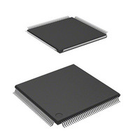
DF2161BVTE10 Renesas Electronics America, DF2161BVTE10 Datasheet - Page 538

DF2161BVTE10
Manufacturer Part Number
DF2161BVTE10
Description
MCU 3V 128K 144-TQFP
Manufacturer
Renesas Electronics America
Series
H8® H8S/2100r
Datasheet
1.DF2160BVT10V.pdf
(847 pages)
Specifications of DF2161BVTE10
Core Processor
H8S/2000
Core Size
16-Bit
Speed
10MHz
Connectivity
Host Interface (LPC), I²C, IrDA, SCI, X-Bus
Peripherals
PWM, WDT
Number Of I /o
114
Program Memory Size
128KB (128K x 8)
Program Memory Type
FLASH
Ram Size
4K x 8
Voltage - Supply (vcc/vdd)
2.7 V ~ 3.6 V
Data Converters
A/D 8x10b; D/A 2x8b
Oscillator Type
Internal
Operating Temperature
-20°C ~ 75°C
Package / Case
144-TQFP, 144-VQFP
Lead Free Status / RoHS Status
Contains lead / RoHS non-compliant
Eeprom Size
-
Other names
HD64F2161BVTE10
HD64F2161BVTE10
HD64F2161BVTE10
- Current page: 538 of 847
- Download datasheet (5Mb)
Section 16 I
9. Note on when I
Note: This restriction on usage can be canceled by setting the FNC1 and FNC0 bits to 1 in
Rev. 3.00 Mar 21, 2006 page 482 of 788
REJ09B0300-0300
In cases where the rise time of the 9th clock of SCL exceeds the stipulated value because of a
large bus load capacity or where a slave device in which a wait can be inserted by driving the
SCL pin low is used, the stop condition instruction should be issued after reading SCL after the
rise of the 9th clock pulse and determining that it is low.
ICXR.
SDA
IRIC
SCL
2
C Bus Interface (IIC) (Optional)
2
C bus interface stop condition instruction is issued
VIH
9th clock
Figure 16.32 Stop Condition Issuance Timing
SCL is detected as low
because the rise of the
waveform is delayed
[1] SCL = low determination
Secures a high period
[2] Stop condition instruction issuance
Stop condition generation
Related parts for DF2161BVTE10
Image
Part Number
Description
Manufacturer
Datasheet
Request
R

Part Number:
Description:
KIT STARTER FOR M16C/29
Manufacturer:
Renesas Electronics America
Datasheet:

Part Number:
Description:
KIT STARTER FOR R8C/2D
Manufacturer:
Renesas Electronics America
Datasheet:

Part Number:
Description:
R0K33062P STARTER KIT
Manufacturer:
Renesas Electronics America
Datasheet:

Part Number:
Description:
KIT STARTER FOR R8C/23 E8A
Manufacturer:
Renesas Electronics America
Datasheet:

Part Number:
Description:
KIT STARTER FOR R8C/25
Manufacturer:
Renesas Electronics America
Datasheet:

Part Number:
Description:
KIT STARTER H8S2456 SHARPE DSPLY
Manufacturer:
Renesas Electronics America
Datasheet:

Part Number:
Description:
KIT STARTER FOR R8C38C
Manufacturer:
Renesas Electronics America
Datasheet:

Part Number:
Description:
KIT STARTER FOR R8C35C
Manufacturer:
Renesas Electronics America
Datasheet:

Part Number:
Description:
KIT STARTER FOR R8CL3AC+LCD APPS
Manufacturer:
Renesas Electronics America
Datasheet:

Part Number:
Description:
KIT STARTER FOR RX610
Manufacturer:
Renesas Electronics America
Datasheet:

Part Number:
Description:
KIT STARTER FOR R32C/118
Manufacturer:
Renesas Electronics America
Datasheet:

Part Number:
Description:
KIT DEV RSK-R8C/26-29
Manufacturer:
Renesas Electronics America
Datasheet:

Part Number:
Description:
KIT STARTER FOR SH7124
Manufacturer:
Renesas Electronics America
Datasheet:

Part Number:
Description:
KIT STARTER FOR H8SX/1622
Manufacturer:
Renesas Electronics America
Datasheet:

Part Number:
Description:
KIT DEV FOR SH7203
Manufacturer:
Renesas Electronics America
Datasheet:


