MC9S12XEP100MAL Freescale Semiconductor, MC9S12XEP100MAL Datasheet - Page 1204
MC9S12XEP100MAL
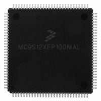
Manufacturer Part Number
MC9S12XEP100MAL
Description
IC MCU 16BIT 1M FLASH 112-LQFP
Manufacturer
Freescale Semiconductor
Series
HCS12r
Datasheet
1.MC9S12XEP768CAL.pdf
(1328 pages)
Specifications of MC9S12XEP100MAL
Core Processor
HCS12X
Core Size
16-Bit
Speed
50MHz
Connectivity
CAN, EBI/EMI, I²C, IrDA, SCI, SPI
Peripherals
LVD, POR, PWM, WDT
Number Of I /o
91
Program Memory Size
1MB (1M x 8)
Program Memory Type
FLASH
Eeprom Size
4K x 8
Ram Size
64K x 8
Voltage - Supply (vcc/vdd)
1.72 V ~ 5.5 V
Data Converters
A/D 16x12b
Oscillator Type
External
Operating Temperature
-40°C ~ 125°C
Package / Case
112-LQFP
Processor Series
S12XE
Core
HCS12
Data Bus Width
16 bit
Data Ram Size
64 KB
Interface Type
SPI, SSI
Maximum Clock Frequency
50 MHz
Number Of Programmable I/os
91
Number Of Timers
25
Operating Supply Voltage
- 0.3 V to + 6 V
Maximum Operating Temperature
+ 105 C
Mounting Style
SMD/SMT
3rd Party Development Tools
EWHCS12
Development Tools By Supplier
KIT33812ECUEVME, EVB9S12XEP100, DEMO9S12XEP100
Minimum Operating Temperature
- 40 C
On-chip Adc
10 bit, 16 Channel
For Use With
EVB9S12XEP100 - BOARD EVAL FOR MC9S12XEP100DEMO9S12XEP100 - BOARD DEMO FOR MC9S12XEP100
Lead Free Status / RoHS Status
Lead free / RoHS Compliant
Available stocks
Company
Part Number
Manufacturer
Quantity
Price

Company:
Part Number:
MC9S12XEP100MAL
Manufacturer:
Freescale Semiconductor
Quantity:
10 000
Part Number:
MC9S12XEP100MAL
Manufacturer:
FREESCALE
Quantity:
20 000


Appendix A Electrical Characteristics
The VDDF
The VDD, VSS2 are the supply pins for the internal digital logic.
VDDPLL, VSSPLL pin pair supply the oscillator and the PLL.
VSS1, VSS2 and VSS3 are internally connected by metal.
VDDA1, and VDDA2 are internally connected by metal.
All VDDX pins are internally connected by metal.
All VSSX pins are internally connected by metal.
VDDA is connected to all VDDX pins by diodes for ESD protection such that VDDX must not exceed
VDDA by more than a diode voltage drop. VDDA can exceed VDDX by more than a diode drop in order
to support applications with a 5V A/D converter range and 3.3V I/O pin range.
VSSA and VSSX are connected by anti-parallel diodes for ESD protection.
A.1.3
There are four groups of functional pins.
A.1.3.1
Standard I/O pins have a level in the range of 3.13V to 5.5 V. This class of pins is comprised of all port I/O
pins (including PortAD), BKGD and the RESET pins.The internal structure of all those pins is identical;
however, some of the functionality may be disabled. For example the BKGD pin pull up is always enabled.
A.1.3.2
This group is made up by the V
1204
,
Pins
VSS1 pin pair supplies the internal NVM logic.
I/O Pins
Analog Reference
Connecting VDDR to VSS disables the internal voltage regulator.
In the following context V
VDDX; V
I
pins. The Run mode current in the VDDX domain is external load
dependent.
V
V
I
VDDPLL.
DD35
DD
DD
DDPLL
is used for the sum of the currents flowing into VDD, VDDF and
is used for VDD, V
denotes the sum of the currents flowing into the VDDA and VDDR
is used for VDDPLL, V
SS35
is used for either VSSA and VSSX unless otherwise noted.
MC9S12XE-Family Reference Manual , Rev. 1.23
RH
and V
SS
RL
DD35
is used for VSS1, VSS2 and VSS3.
pins.
is used for either VDDA, VDDR, and
SSPLL
NOTE
NOTE
is used for VSSPLL
Freescale Semiconductor
Related parts for MC9S12XEP100MAL
Image
Part Number
Description
Manufacturer
Datasheet
Request
R

Part Number:
Description:
Manufacturer:
Freescale Semiconductor, Inc
Datasheet:
Part Number:
Description:
Manufacturer:
Freescale Semiconductor, Inc
Datasheet:
Part Number:
Description:
Manufacturer:
Freescale Semiconductor, Inc
Datasheet:
Part Number:
Description:
Manufacturer:
Freescale Semiconductor, Inc
Datasheet:
Part Number:
Description:
Manufacturer:
Freescale Semiconductor, Inc
Datasheet:
Part Number:
Description:
Manufacturer:
Freescale Semiconductor, Inc
Datasheet:
Part Number:
Description:
Manufacturer:
Freescale Semiconductor, Inc
Datasheet:
Part Number:
Description:
Manufacturer:
Freescale Semiconductor, Inc
Datasheet:
Part Number:
Description:
Manufacturer:
Freescale Semiconductor, Inc
Datasheet:
Part Number:
Description:
Manufacturer:
Freescale Semiconductor, Inc
Datasheet:
Part Number:
Description:
Manufacturer:
Freescale Semiconductor, Inc
Datasheet:
Part Number:
Description:
Manufacturer:
Freescale Semiconductor, Inc
Datasheet:
Part Number:
Description:
Manufacturer:
Freescale Semiconductor, Inc
Datasheet:
Part Number:
Description:
Manufacturer:
Freescale Semiconductor, Inc
Datasheet:
Part Number:
Description:
Manufacturer:
Freescale Semiconductor, Inc
Datasheet: