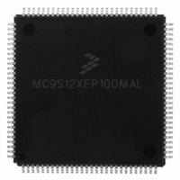
MC9S12XEP100MAL Freescale Semiconductor, MC9S12XEP100MAL Datasheet - Page 510

MC9S12XEP100MAL
Manufacturer Part Number
MC9S12XEP100MAL
Description
IC MCU 16BIT 1M FLASH 112-LQFP
Manufacturer
Freescale Semiconductor
Series
HCS12r
Datasheet
1.MC9S12XEP768CAL.pdf
(1328 pages)
Specifications of MC9S12XEP100MAL
Core Processor
HCS12X
Core Size
16-Bit
Speed
50MHz
Connectivity
CAN, EBI/EMI, I²C, IrDA, SCI, SPI
Peripherals
LVD, POR, PWM, WDT
Number Of I /o
91
Program Memory Size
1MB (1M x 8)
Program Memory Type
FLASH
Eeprom Size
4K x 8
Ram Size
64K x 8
Voltage - Supply (vcc/vdd)
1.72 V ~ 5.5 V
Data Converters
A/D 16x12b
Oscillator Type
External
Operating Temperature
-40°C ~ 125°C
Package / Case
112-LQFP
Processor Series
S12XE
Core
HCS12
Data Bus Width
16 bit
Data Ram Size
64 KB
Interface Type
SPI, SSI
Maximum Clock Frequency
50 MHz
Number Of Programmable I/os
91
Number Of Timers
25
Operating Supply Voltage
- 0.3 V to + 6 V
Maximum Operating Temperature
+ 105 C
Mounting Style
SMD/SMT
3rd Party Development Tools
EWHCS12
Development Tools By Supplier
KIT33812ECUEVME, EVB9S12XEP100, DEMO9S12XEP100
Minimum Operating Temperature
- 40 C
On-chip Adc
10 bit, 16 Channel
For Use With
EVB9S12XEP100 - BOARD EVAL FOR MC9S12XEP100DEMO9S12XEP100 - BOARD DEMO FOR MC9S12XEP100
Lead Free Status / RoHS Status
Lead free / RoHS Compliant
Available stocks
Company
Part Number
Manufacturer
Quantity
Price
Company:
Part Number:
MC9S12XEP100MAL
Manufacturer:
Freescale Semiconductor
Quantity:
10 000
Part Number:
MC9S12XEP100MAL
Manufacturer:
FREESCALE
Quantity:
20 000
- Current page: 510 of 1328
- Download datasheet (9Mb)
Chapter 13 Analog-to-Digital Converter (ADC12B16CV1)
13.3.2
This section describes in address order all the ADC12B16C registers and their individual bits.
13.3.2.1
Writes to this register will abort current conversion sequence.
Read: Anytime
Write: Anytime, in special modes always write 0 to Reserved Bit 7.
510
Address
0x002C
Module Base + 0x0000
0x0024
0x0026
0x0028
0x002A
0x002E
WRAP[3-0]
Because of an order from the United States International Trade Commission, BGA-packaged product lines and partnumbers
Reset
indicated here currently are not available from Freescale for import or sale in the United States prior to September 2010
Field
3-0
W
R
ATDDR10
ATDDR11
ATDDR12
ATDDR13
ATDDR14
ATDDR15
Reserved
Register Descriptions
Name
Wrap Around Channel Select Bits — These bits determine the channel for wrap around when doing multi-
channel conversions. The coding is summarized in
ATD Control Register 0 (ATDCTL0)
0
7
WRAP3 WRAP2 WRAP1 WRAP0
0
= Unimplemented or Reserved
W
W
W
W
W
W
R
R
R
R
R
R
Figure 13-2. ADC12B16C Register Summary (Sheet 3 of 3)
0
0
6
Bit 7
0
Table 13-3. Multi-Channel Wrap Around Coding
Figure 13-3. ATD Control Register 0 (ATDCTL0)
MC9S12XE-Family Reference Manual , Rev. 1.23
Table 13-2. ATDCTL0 Field Descriptions
= Unimplemented or Reserved
0
5
0
0
and
and
and
and
and
and
6
See
See
See
See
See
See
Section 13.3.2.12.2, “Right Justified Result Data (DJM=1)”
Section 13.3.2.12.2, “Right Justified Result Data (DJM=1)”
Section 13.3.2.12.2, “Right Justified Result Data (DJM=1)”
Section 13.3.2.12.2, “Right Justified Result Data (DJM=1)”
Section 13.3.2.12.2, “Right Justified Result Data (DJM=1)”
Section 13.3.2.12.2, “Right Justified Result Data (DJM=1)”
Section 13.3.2.12.1, “Left Justified Result Data (DJM=0)”
Section 13.3.2.12.1, “Left Justified Result Data (DJM=0)”
Section 13.3.2.12.1, “Left Justified Result Data (DJM=0)”
Section 13.3.2.12.1, “Left Justified Result Data (DJM=0)”
Section 13.3.2.12.1, “Left Justified Result Data (DJM=0)”
Section 13.3.2.12.1, “Left Justified Result Data (DJM=0)”
0
5
0
0
4
Multiple Channel Conversions (MULT = 1)
Description
Wraparound to AN0 after Converting
Table
4
WRAP3
13-3.
1
3
Reserved
3
WRAP2
(1)
2
1
2
WRAP1
Freescale Semiconductor
1
1
1
WRAP0
Bit 0
1
0
Related parts for MC9S12XEP100MAL
Image
Part Number
Description
Manufacturer
Datasheet
Request
R
Part Number:
Description:
Manufacturer:
Freescale Semiconductor, Inc
Datasheet:
Part Number:
Description:
Manufacturer:
Freescale Semiconductor, Inc
Datasheet:
Part Number:
Description:
Manufacturer:
Freescale Semiconductor, Inc
Datasheet:
Part Number:
Description:
Manufacturer:
Freescale Semiconductor, Inc
Datasheet:
Part Number:
Description:
Manufacturer:
Freescale Semiconductor, Inc
Datasheet:
Part Number:
Description:
Manufacturer:
Freescale Semiconductor, Inc
Datasheet:
Part Number:
Description:
Manufacturer:
Freescale Semiconductor, Inc
Datasheet:
Part Number:
Description:
Manufacturer:
Freescale Semiconductor, Inc
Datasheet:
Part Number:
Description:
Manufacturer:
Freescale Semiconductor, Inc
Datasheet:
Part Number:
Description:
Manufacturer:
Freescale Semiconductor, Inc
Datasheet:
Part Number:
Description:
Manufacturer:
Freescale Semiconductor, Inc
Datasheet:
Part Number:
Description:
Manufacturer:
Freescale Semiconductor, Inc
Datasheet:
Part Number:
Description:
Manufacturer:
Freescale Semiconductor, Inc
Datasheet:
Part Number:
Description:
Manufacturer:
Freescale Semiconductor, Inc
Datasheet:
Part Number:
Description:
Manufacturer:
Freescale Semiconductor, Inc
Datasheet:


