HD64F2638F20J Renesas Electronics America, HD64F2638F20J Datasheet - Page 270
HD64F2638F20J
Manufacturer Part Number
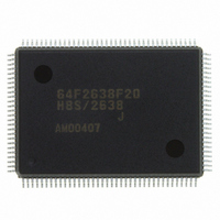
HD64F2638F20J
Description
IC H8S MCU FLASH 256K 128-QFP
Manufacturer
Renesas Electronics America
Series
H8® H8S/2600r
Specifications of HD64F2638F20J
Core Processor
H8S/2600
Core Size
16-Bit
Speed
20MHz
Connectivity
CAN, SCI, SmartCard
Peripherals
Motor Control PWM, POR, PWM, WDT
Number Of I /o
72
Program Memory Size
256KB (256K x 8)
Program Memory Type
FLASH
Ram Size
16K x 8
Voltage - Supply (vcc/vdd)
4.5 V ~ 5.5 V
Data Converters
A/D 12x10b; D/A 2x8b
Oscillator Type
Internal
Operating Temperature
-40°C ~ 85°C
Package / Case
128-QFP
Lead Free Status / RoHS Status
Contains lead / RoHS non-compliant
Eeprom Size
-
Available stocks
Company
Part Number
Manufacturer
Quantity
Price
Company:

Part Number:
HD64F2638F20J
Manufacturer:
PENESAS
Quantity:
252


Section 8 Data Transfer Controller (DTC)
[10] When the specified number of transfers are completed (the TPU transfer CRA value is 0), the
(3) Software Activation
An example is shown in which the DTC is used to transfer a block of 128 bytes of data by means
of software activation. The transfer source address is H'1000 and the destination address is
H'2000. The vector number is H'60, so the vector address is H'04C0.
[1] Set MRA to incrementing source address (SM1 = 1, SM0 = 0), incrementing destination
[2] Set the start address of the register information at the DTC vector address (H'04C0).
[3] Check that the SWDTE bit in DTVECR is 0. Check that there is currently no transfer activated
[4] Write 1 to the SWDTE bit and the vector number (H'60) to DTVECR. The write data is H'E0.
[5] Read DTVECR again and check that it is set to the vector number (H'60). If it is not, this
[6] If the write was successful, the DTC is activated and a block of 128 bytes of data is transferred.
[7] After the transfer, an SWDTEND interrupt occurs. The interrupt handling routine should clear
Page 220 of 1458
address (DM1 = 1, DM0 = 0), block transfer mode (MD1 = 1, MD0 = 0), and byte size (Sz =
0). The DTS bit can have any value. Set MRB for one block transfer by one interrupt (CHNE =
0). Set the transfer source address (H'1000) in SAR, the destination address (H'2000) in DAR,
and 128 (H'8080) in CRA. Set 1 (H'0001) in CRB.
by software.
indicates that the write failed. This is presumably because an interrupt occurred between steps
3 and 4 and led to a different software activation. To activate this transfer, go back to step 3.
the SWDTE bit to 0 and perform other wrap-up processing.
TGFA flag is held at 1, the DTCE bit is cleared to 0, and a TGIA interrupt request is sent to
the CPU. Termination processing should be performed in the interrupt handling routine.
H8S/2639, H8S/2638, H8S/2636,
REJ09B0103-0800 Rev. 8.00
H8S/2630, H8S/2635 Group
May 28, 2010
Related parts for HD64F2638F20J
Image
Part Number
Description
Manufacturer
Datasheet
Request
R


Part Number:
Description:
KIT STARTER FOR M16C/29
Manufacturer:
Renesas Electronics America
Datasheet:

Part Number:
Description:
KIT STARTER FOR R8C/2D
Manufacturer:
Renesas Electronics America
Datasheet:

Part Number:
Description:
R0K33062P STARTER KIT
Manufacturer:
Renesas Electronics America
Datasheet:

Part Number:
Description:
KIT STARTER FOR R8C/23 E8A
Manufacturer:
Renesas Electronics America
Datasheet:

Part Number:
Description:
KIT STARTER FOR R8C/25
Manufacturer:
Renesas Electronics America
Datasheet:

Part Number:
Description:
KIT STARTER H8S2456 SHARPE DSPLY
Manufacturer:
Renesas Electronics America
Datasheet:

Part Number:
Description:
KIT STARTER FOR R8C38C
Manufacturer:
Renesas Electronics America
Datasheet:

Part Number:
Description:
KIT STARTER FOR R8C35C
Manufacturer:
Renesas Electronics America
Datasheet:

Part Number:
Description:
KIT STARTER FOR R8CL3AC+LCD APPS
Manufacturer:
Renesas Electronics America
Datasheet:
Part Number:
Description:
KIT STARTER FOR RX610
Manufacturer:
Renesas Electronics America
Datasheet:

Part Number:
Description:
KIT STARTER FOR R32C/118
Manufacturer:
Renesas Electronics America
Datasheet:

Part Number:
Description:
KIT DEV RSK-R8C/26-29
Manufacturer:
Renesas Electronics America
Datasheet:

Part Number:
Description:
KIT STARTER FOR SH7124
Manufacturer:
Renesas Electronics America
Datasheet:

Part Number:
Description:
KIT STARTER FOR H8SX/1622
Manufacturer:
Renesas Electronics America
Datasheet: