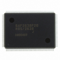
HD64F2638F20J Renesas Electronics America, HD64F2638F20J Datasheet - Page 589

HD64F2638F20J
Manufacturer Part Number
HD64F2638F20J
Description
IC H8S MCU FLASH 256K 128-QFP
Manufacturer
Renesas Electronics America
Series
H8® H8S/2600r
Specifications of HD64F2638F20J
Core Processor
H8S/2600
Core Size
16-Bit
Speed
20MHz
Connectivity
CAN, SCI, SmartCard
Peripherals
Motor Control PWM, POR, PWM, WDT
Number Of I /o
72
Program Memory Size
256KB (256K x 8)
Program Memory Type
FLASH
Ram Size
16K x 8
Voltage - Supply (vcc/vdd)
4.5 V ~ 5.5 V
Data Converters
A/D 12x10b; D/A 2x8b
Oscillator Type
Internal
Operating Temperature
-40°C ~ 85°C
Package / Case
128-QFP
Lead Free Status / RoHS Status
Contains lead / RoHS non-compliant
Eeprom Size
-
Available stocks
Company
Part Number
Manufacturer
Quantity
Price
Company:
Part Number:
HD64F2638F20J
Manufacturer:
PENESAS
Quantity:
252
- Current page: 589 of 1512
- Download datasheet (9Mb)
H8S/2639, H8S/2638, H8S/2636,
H8S/2630, H8S/2635 Group
In a receive operation, an RXI interrupt request is generated when the RDRF flag in SSR is set to
1. If the RXI request is designated beforehand as a DTC activation source, the DTC will be
activated by the RXI request, and transfer of the receive data will be carried out. The RDRF flag is
cleared to 0 automatically when data transfer is performed by the DTC. If an error occurs, an error
flag is set but the RDRF flag is not. Consequently, the DTC is not activated, but instead, an ERI
interrupt request is sent to the CPU. Therefore, the error flag should be cleared.
Notes: For block transfer mode, see section 13.4, SCI Interrupts.
14.3.7
Switching the Mode: When switching between smart card interface mode and software standby
mode, the following switching procedure should be followed in order to maintain the clock duty.
• When changing from smart card interface mode to software standby mode
[1] Set the data register (DR) and data direction register (DDR) corresponding to the SCK pin to
[2] Write 0 to the TE bit and RE bit in the serial control register (SCR) to halt transmit/receive
[3] Write 0 to the CKE0 bit in SCR to halt the clock.
[4] Wait for one serial clock period.
[5] Make the transition to the software standby state.
• When returning to smart card interface mode from software standby mode
[6] Exit the software standby state.
[7] Write 1 to the CKE0 bit in SCR and output the clock. Signal generation is started with the
REJ09B0103-0800 Rev. 8.00
May 28, 2010
the value for the fixed output state in software standby mode.
operation. At the same time, set the CKE1 bit to the value for the fixed output state in software
standby mode.
During this interval, clock output is fixed at the specified level, with the duty preserved.
normal duty.
* The DTC is not implemented in the H8S/2635 Group.
Operation in GSM Mode
Section 14 Smart Card Interface
Page 539 of 1458
Related parts for HD64F2638F20J
Image
Part Number
Description
Manufacturer
Datasheet
Request
R

Part Number:
Description:
KIT STARTER FOR M16C/29
Manufacturer:
Renesas Electronics America
Datasheet:

Part Number:
Description:
KIT STARTER FOR R8C/2D
Manufacturer:
Renesas Electronics America
Datasheet:

Part Number:
Description:
R0K33062P STARTER KIT
Manufacturer:
Renesas Electronics America
Datasheet:

Part Number:
Description:
KIT STARTER FOR R8C/23 E8A
Manufacturer:
Renesas Electronics America
Datasheet:

Part Number:
Description:
KIT STARTER FOR R8C/25
Manufacturer:
Renesas Electronics America
Datasheet:

Part Number:
Description:
KIT STARTER H8S2456 SHARPE DSPLY
Manufacturer:
Renesas Electronics America
Datasheet:

Part Number:
Description:
KIT STARTER FOR R8C38C
Manufacturer:
Renesas Electronics America
Datasheet:

Part Number:
Description:
KIT STARTER FOR R8C35C
Manufacturer:
Renesas Electronics America
Datasheet:

Part Number:
Description:
KIT STARTER FOR R8CL3AC+LCD APPS
Manufacturer:
Renesas Electronics America
Datasheet:

Part Number:
Description:
KIT STARTER FOR RX610
Manufacturer:
Renesas Electronics America
Datasheet:

Part Number:
Description:
KIT STARTER FOR R32C/118
Manufacturer:
Renesas Electronics America
Datasheet:

Part Number:
Description:
KIT DEV RSK-R8C/26-29
Manufacturer:
Renesas Electronics America
Datasheet:

Part Number:
Description:
KIT STARTER FOR SH7124
Manufacturer:
Renesas Electronics America
Datasheet:

Part Number:
Description:
KIT STARTER FOR H8SX/1622
Manufacturer:
Renesas Electronics America
Datasheet:


